
Introduction to FPGAs
source link: https://smist08.wordpress.com/2023/02/04/introduction-to-fpgas/
Go to the source link to view the article. You can view the picture content, updated content and better typesetting reading experience. If the link is broken, please click the button below to view the snapshot at that time.
Introduction
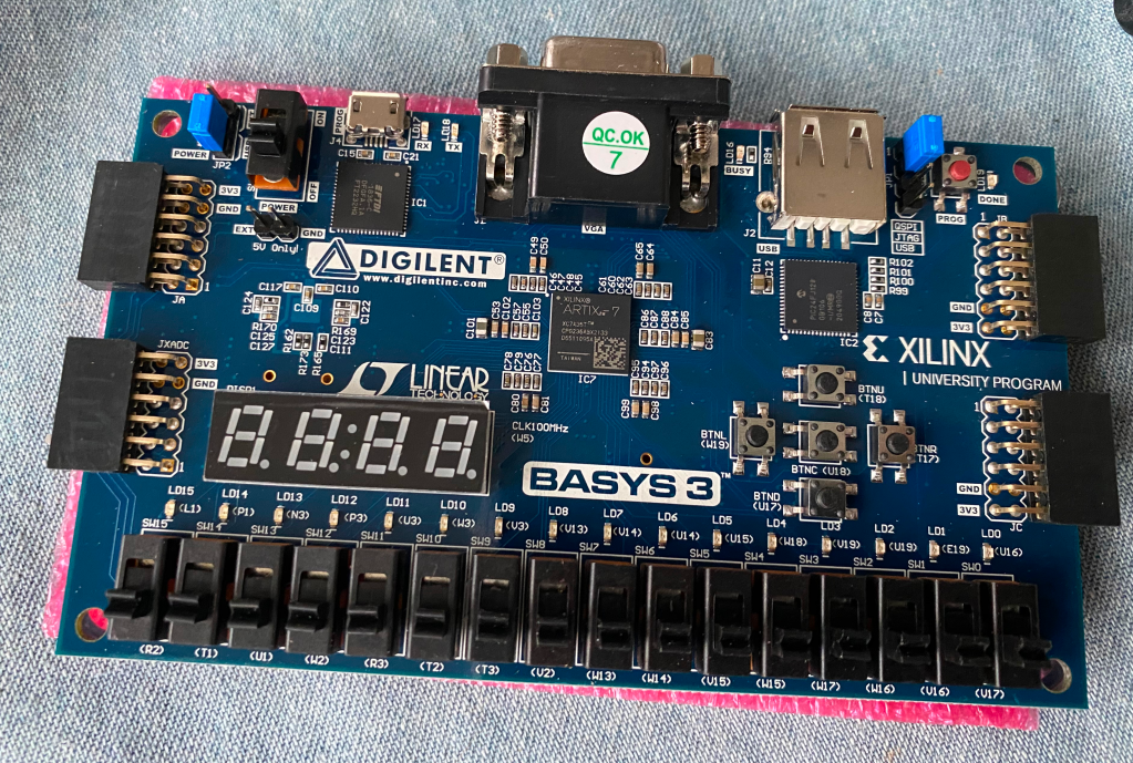
Field Programmable Gate Arrays (FPGAs) are a form of programmable hardware that has become inexpensive and accessible recently. I recently purchased a Digilent Basys 3 FPGA development board for $200 based on a Xilinx Artix-7 FPGA. Xilinx makes their development software available free for non-commercial use on these lower end chips. If you’ve ever been interested in how chips are designed and developed, then FPGAs are a great way to get started. You program FPGAs using the same hardware design software that is used to design custom integrated circuit chips (ASICs). In this post, we’ll start to look at what an FPGA is and how it works.
Logic Gates and Truth Tables
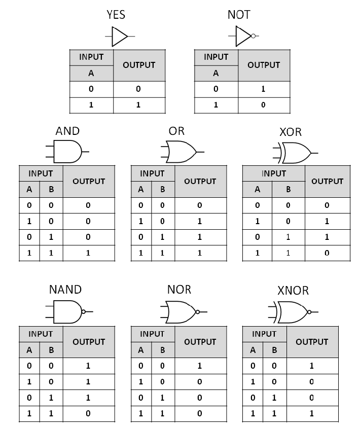
Anyone that has taken a basic logic course will have encountered truth tables for the basic logic operations. Below are the basic logic building blocks including their symbol and truth table.
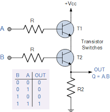
You can then build complicated logic circuits out of these building blocks. If you want to build an I/C, then you use a design pattern of the transistors for each logic gate. For instance a possible AND gate made out of transistors and resistors is below.
To build a CPU, you need a few more elements than basic logic gates, namely memory and a way to synchronize everything to a clock, but this is a good starting point.
FPGAs
The basic idea behind an FPGA is to provide an array of circuit elements that can execute any truth table, or lookup table in FPGA parlance. You program the FPGA by downloading all the truth tables to it and then execute them. A Xilinx Artix-7 FPGA contains thousands of configurable logic blocks (CLBs), each of which can be configured to execute a single 6-input lookup table (LUT) or two 5-input LUTs.
When you start building arithmetic operations from basic logic elements, you need a carry output as well. The CLBs support carry out operations so you can implement circuits like full adders. Further some of the CLBs contain memory and shift registers that you can use.
Extras
As chip densities and transistor counts increase, FPGA can have quite a large number of CLBs on a single chip. Further other elements are added to optimize common operations. For instance performing multiplication using the tools described is possible, but quite slow. Most FPGAs now contain custom multipliers that can be configured in or even a DSP. Similarly most FPGAs have custom components for external interfaces such as USB or I2C.
Programming
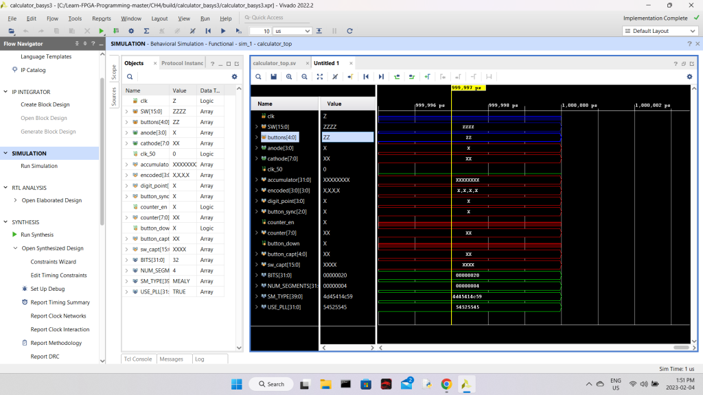
FPGAs are programmed using hardware description languages such as SystemVerilog or VHDL. Both of these compile to what is required for your development board. The cool thing is that this same HDL could be used to generate the layout/masking for a custom application specific I/C (ASIC). The Xilinix development environment is Vivado which supports writing and compiling your HDL along with creating testbenches and running simulations. It also has limited debug support for running on your development board. Here is the source code view:
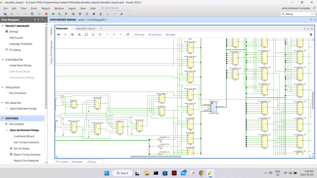
Here is the generated circuit diagram:
Here we run a simulation and can study the timing diagram:
The thing to remember is that HDL describes hardware and even though it looks like a programming language, it only superficially behaves like a programming language.
Why FPGAs?
FPGAs typically run at 300MHz or so. This is well below the speed of typical ARM, Intel or AMD CPUs. The big advantage of FPGAs is getting something up and running quickly using an iterative development/debug cycle. If you are creating ASICs then you need to do the design, send them out for test manufacturing and then test what you get back, a slow and expensive process.
For instance, a lot of the first RISC-V CPUs on the market were implemented on FPGAs. This is why they usually have fewer CPU cores and run at around 300MHz. This brought them to market quickly to let people start writing RISC-V code, such as adding basic support for RISC-V in the GCC compiler and the Linux kernel.
Another advantage of FPGAs is that if there is a bug, you can reprogram them. FPGAs are commonly used in automobiles and this allows the manufacturers to change the hardware via software updates rather than executing a costly recall and having to replace ASICs or circuit boards.
The other thing to note when implementing in hardware, like with FPGAs, is that you have a much greater freedom to run things in parallel. In fact everything runs at once by default, and you have to do some work to synchronize or serialize operations. This allows you to develop highly parallel processes, like for GPUs or TPUs. This level of parallelism gives FPGA development a huge advantage over CPUs and traditional programming, for certain application areas.
Summary
If you are interested in how I/Cs or CPUs are designed and implemented then inexpensive FPGA boards from companies like Digilent are a great starting point. The cost of entry is minimal and even if the hardware is lower end by today’s standards, it still gives you a long runway for learning. A great diversion for DIY electronics hobbyists.
Recommend
About Joyk
Aggregate valuable and interesting links.
Joyk means Joy of geeK
