

Nibbler 4 Bit CPU
source link: https://www.bigmessowires.com/nibbler/
Go to the source link to view the article. You can view the picture content, updated content and better typesetting reading experience. If the link is broken, please click the button below to view the snapshot at that time.
Summary
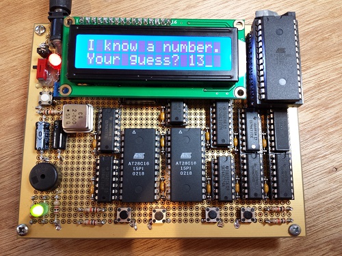
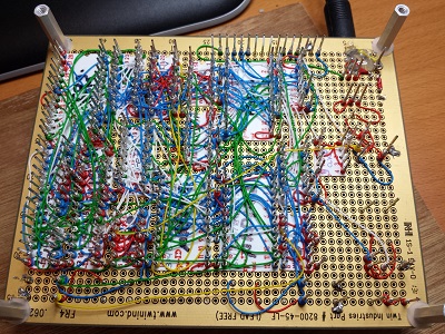
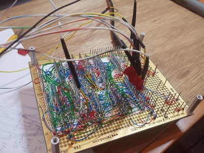
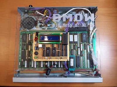
Nibbler is a 4 bit CPU built from standard 7400 series logic chips – individual counters, registers, buffers, and gates. It’s an educational example of a simple CPU that’s easy to understand and build, but still capable of running games and other interesting programs. Nibbler is built using wire-wrapping on a 5 x 4 inch (127 x 102 mm) perfboard. The CPU contains 17 chips in total.
Download the Nibbler file archive containing all the design files and tools.
Follow the development history of Nibbler to learn more about the process that led to its construction.
Specs
- 4 bit custom-made CPU
- 12 bit addressing, 4K address space size
- Harvard architecture – separate program and data memory spaces
- 2.46 MHz clock speed, 2 clocks per instruction = 1.23 million instructions/sec
- Thirteen 7400-series chips in the CPU data and control paths
- Two 28C16 EEPROMs store microcode for generating internal control signals
- 4K x 4 SRAM (CY7C168A)
- 28C64 EEPROM stores programs
- Four pushbutton inputs
- 16 x 2 character LCD
- Audio speaker
- About 100 mA current draw at 5V
Demos
For a small pile of 7400 logic chips, Nibbler can do some cool stuff! Check out these videos of Nibbler running the games Mastermind and Frogger, and playing the Blue Danube Waltz. For lots more information about how these demos were made, see this post. Switch to the 480p quality setting for a bit more detail in the videos.
Architecture
The primary design goal was to make everything easy to understand, to encourage other people to learn from Nibbler and get inspired to build their own CPU. In several cases, obvious performance optimizations were intentionally omitted in order to keep things simple. However, Nibbler is not a true minimal CPU. With a 12-bit address space and a 16 x 2 character LCD display, it’s capable of much more than just blinking a few LEDs.
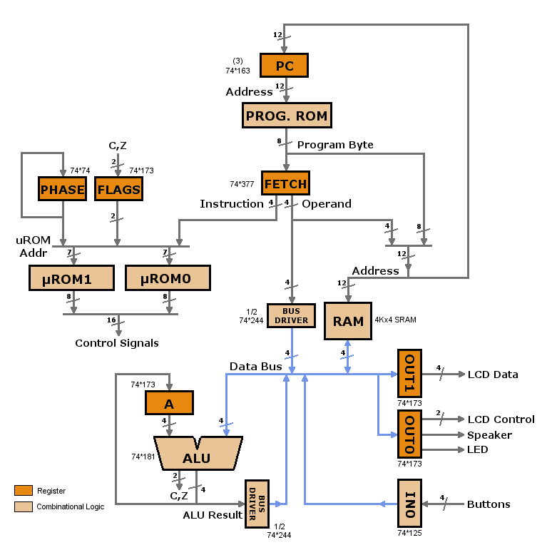
The architecture of Nibbler is shown above. The program counter (PC) provides the address for the program ROM. The program byte is combined with other status bits to provide the address for the microcode ROMs. These ROMs generate the internal control signals needed to load, enable, and increment the other chips in the CPU at the appropriate times. Each ROM outputs a different set of eight of the sixteen total control signals. The program byte is also used to construct addresses for RAM and for jump destinations, as well as to put immediate literal values on the data bus.
In contrast to most modern CPUs, the Nibbler design uses a Harvard Architecture. That means programs and data are stored in separate address spaces, and travel on separate busses. The data bus is 4 bits wide, as one should expect for a 4-bit CPU. The program bus is 8 bits wide: 4 bits for the instruction opcode, and 4 bits for the immediate operand or high bits of the target address.
Because instruction opcodes are 4 bits wide, there are 16 possible types of instructions. All instructions require exactly two clock cycles to execute. During the first clock cycle, called phase 0, the instruction opcode and operand are retrieved from memory and stored in a register called Fetch. The second clock cycle, called phase 1, performs the calculation or operation needed to execute the instruction.
A load-store design is used, with all arithmetic and logical computation results stored into the single 4-bit accumulator register named “A”. Data can be moved between A and memory locations in RAM, but otherwise all the CPU instructions operate only on A.
Program and data addresses are both 12 bits wide, resulting in total addressable storage of 4096 8-bit bytes for programs and 4096 4-bit nibbles for data. Since instruction opcodes are 4 bits wide, instructions involving absolute memory addresses are 4 + 12 = 16 bits in size, or two program bytes. Instructions involving only a 4 bit literal value are 4 + 4 = 8 bits in size, or one program byte.
Up to thirty-two distinct I/O devices can be supported by the design: sixteen inputs and sixteen outputs. However, Nibbler uses just one IN port and two OUT ports. The input comes from four momentary pushbuttons, arranged in a left/right/down/up configuration, and connected to the lone IN port. Output utilizes one of the two OUT ports, and includes a programmer LED used for debugging, as well as a piezo speaker for software-controlled sound, and a 16 x 2 character-based LCD display.
Limitations
Nibbler is notable for a few things it does NOT have. There’s no address decoder, because there’s not more than one chip mapped into different regions of the same address space. Program ROM occupies all of the program address space, and RAM occupies all of the data address space. I/O peripherals aren’t memory-mapped, but instead use port-specific IN and OUT instructions to transfer data.
Nibbler also lacks any address registers, which means it can’t support any form of indirect addressing, nor a hardware-controlled stack. All memory references must use absolute addresses. That’s a significant limitation, but it’s in keeping with the project’s K.I.S.S. design goals. With the use of jump tables and dedicated memory locations, Nibbler programs can implement a simple call/return mechanism without a true stack.
Schematic
Click the schematic image to view the full-sized version. The whole system fits on a single page, including the CPU itself and the I/O devices, so it’s easy to wrap your head around.
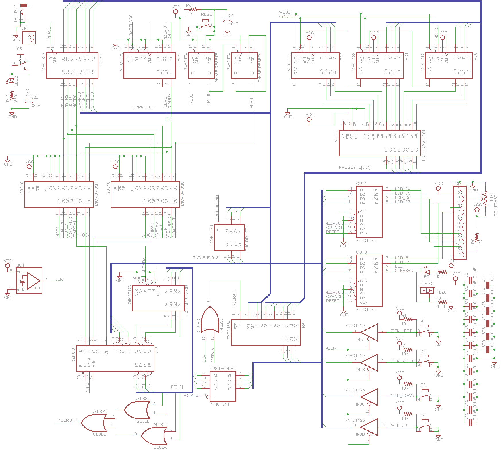
Except for RAM and ROM, all the chips shown here are common 7400 series parts. I used the 7400HCT logic family for most parts, which requires less power while offering similar speed to the more common 7400LS family.
Program Data
The parts on the schematic are arranged in the same relative positions as in the architecture diagram. At the middle-right is the program ROM, where the currently running program is stored. This is an 8Kx8 EEPROM, but Nibbler’s address size only allows for 4K programs, so one of the address inputs is unused and is hard-wired to 0. Program memory is 8 bits wide, and so all 8 of the ROM’s I/O lines are used. Depending on the type of instruction, these may be 4 bits of instruction opcode and 4 bits of immediate operand, or 4 bits of instruction opcode and 4 bits of address, followed by 8 more bits of address. At the start of execution of each instruction, this program byte is loaded into the Fetch register.
The address of the program instruction that’s currently being executed is stored in the program counter. The PC consists of three ’163 4-bit counters, chained together to make a 12 bit logical register. After most instructions, the PC will increment to point to the next instruction. For jump instructions, the PC can also be loaded with a new address. The address comes from the Fetch register operand value (highest 4 bits) and the program ROM byte (lowest 8 bits).
Control and Microcode
At the top left of the schematic are the three chips pertaining to the execution of the current instruction. The Fetch register is a ’377, an 8-bit register that holds the current instruction opcode in the high 4 bits and instruction or address data in the low 4 bits. ALU flags are stored in the 4-bit Flags register, a ’173. There are only two flags, carry and zero, so two of the four bits are unused. The last chip in this group is a ’74, a dual flip-flop. One flip-flop is used to synchronize the reset signal, and another is the Phase bit, which constantly toggles between 0 and 1 to indicate which of the two clock cycles of an instruction’s execution is currently underway. Fetch is loaded at the end of the clock cycle when Phase is 0.
The instruction opcode, ALU flags, and phase are combined to form a 7-bit address for the two microcode ROMs, shown at the mid-left. The output of the two ROMs constitutes the 16 control signals needed to orchestrate the behavior of all the other chips. The microcode is stored in two 2Kx8 EEPROMs, so four of the eleven address inputs on each ROM are unused and hard-wired to 0.
ALU Datapath
At the bottom-left of the schematic are the ’181 ALU and the ’173 accumulator register “A”. The ALU (arithmetic and logic unit) can perform any common arithmetic or logical operation on its two inputs. In this case, one input always comes from the accumulator, while the other is supplied from the data bus. The ALU result is stored back into the accumulator. The ALU, accumulator, and data bus are all 4 bits wide, which is what makes Nibbler a 4 bit CPU.
Carry-In and Carry Flag
If you look carefully, you’ll see that the ALU’s carry-in bit is a control signal provided by microcode, not the carry flag from the Flags register. This is a subtle but important point: the carry flag is an output from an arithmetic instruction, and can be used to make a conditional jump if the carry flag is/isn’t set, but it doesn’t feed back into the ALU to affect later calculations. This means that when performing multi-nibble pair-wise additions, the program must check the carry flag after each nibble addition, and add an extra 1 into the next addition if it’s set.
This was a conscious design choice. If the carry flag did connect to the ALU’s carry-in bit, then the program would need to clear it before performing any single-nibble additions, and those are much more common than multi-nibble additions. Also the carry-in bit can’t simply be hard-wired to 0, because the CMP (compare) instruction requires carry-in to be 1 in order to work properly. So carry-in must be provided by the microcode.
RAM
RAM is shown at the bottom-center. Its I/O lines are connected to the data bus, and the address comes from the Fetch register operand value (highest 4 bits) and the program ROM byte (lowest 8 bits). It’s a 4Kx4 SRAM, to match Nibbler’s address size and data width.
Notice that the CLK signal is OR’d with the /CSRAM control signal, with the result connected to the RAM’s /CS (chip select) input. This means the RAM will only be enabled during the second half of each clock cycle, and even then only when the microcode specifically enables it. This is a simple way of preventing erroneous writes to RAM during the early part of the clock cycle, when the /WE (write enable) signal and RAM address may not yet be valid.
IN and OUT Ports
The IN and OUT ports are also connected to the data bus, and are shown on the schematic at bottom-right. IN0 is a ’125 4-bit bus driver, which outputs the state of four pushbuttons connected to pull-up resistors. Because there’s only a single IN port, no decoding of the port number is done, and this ’125 will actually respond to any port number with the IN instruction. If more IN ports were added, then additional port number decoding logic would be needed.
The two OUT ports are ’173 4 bit registers. OUT1 connects to databus[4..7] of a 16×2 character LCD display using the common HD44780 controller. Although this LCD controller has an 8 bit interface, it can also operate in 4 bit mode, in which case only the highest 4 LCD databus lines are used. OUT0 connects two more lines to the LCD, for the RS and E signals needed to control LCD data transfers. The other two lines from OUT0 connect to an LED, which can be toggled on/off as a basic debugging aid, and to a speaker, which can be bit-banged in software to generate simple square-wave tones at different frequencies.
Notice that the ’173s have two load enable inputs, /G1 and /G2, and both must be low in order to load data to the chip. /G1 of both chips is connected to the /LOADOUT control signal. But as with the IN port, the OUT port number is not fully decoded, in order to avoid needing extra decoding logic. Instead, bit 0 of the port number is connected to OUT0 /G2, and bit 1 to OUT1 /G2. This means that OUT0 will actually respond to any port number where bit 0 is 0, and OUT1 to any port number where bit 1 is 0. It would even be possible to load both OUT ports simultaneously by using a port number where both bits 1 and 0 were 0, although that probably wouldn’t be useful.
Bus Drivers
The last two components on the data bus are a pair of 4-bit bus drivers, shown at the center and at the bottom-center of the schematic. These are two halves of a single ’244 octal driver. One drives the ALU result onto the data bus, which is necessary when storing data to RAM or an OUT port. The other drives the operand value from the Fetch register onto the data bus, which is necessary for instructions that involve an immediate constant value.
Combinatorial Feedback Loops
If you looked carefully at the architecture diagram and the schematics, you may have noticed there’s a combinatorial feedback loop from the ALU output, through bus driver B, and back to the ALU’s B input. If the ALU function were set to something like A + B while bus driver B was enabled, it’s obvious that a feedback problem would be created, as the ALU’s output would also be its input. What’s less obvious is that a feedback loop can be created even if the ALU function is set to A, and the value at input B should be logically irrelevant. Given a closer look at how logic gates are constructed from transistors, you can demonstrate that logically irrelevant doesn’t always mean electrically irrelevant, and a transient invalid voltage on the data bus can lock the ALU into a vicious cycle where invalid input results in invalid output which causes more invalid input. This was a rare problem with the first version of Nibbler, and was discussed in more detail here and here, and finally resolved here.
The feedback loop fix was made in microcode, and relies on knowledge of the internal logic of the SN74LS181, taken from the chip’s datasheet. While unlikely, it’s theoretically possible that a ‘181 from a different logic family or different manufacturer might have a different internal logic for which the microcode-based fix doesn’t work. If you’re building a Nibbler-clone and run into this problem, a Schmitt Trigger buffer like the 74HCT7541 can be placed between the data bus and the ALU’s B input.
Microcode and Instruction Set
Instructions for the Nibbler 4-bit CPU come in two types: immediate and addressed. Both types begin with 4 bits of instruction opcode, to identify the specific instruction. Immediate instructions like ADDI include a 4-bit operand value embedded in the instruction, and so are 8 bits in total size. Addressed instructions like JMP include a 12-bit address in data space (RAM) or program space (ROM), and are 16 bits in total size. The instruction encoding is very simple:
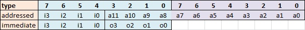
The four instruction opcode bits i[0..3] are combined with the ALU carry flag C and zero flag Z, as well as the Phase bit, in order to form a 7-bit address for the two microcode ROMs. The ROMs’ outputs form the 16 control signals needed to orchestrate the behavior of all the other chips. The contents of the microcode ROMs are shown in the table below.
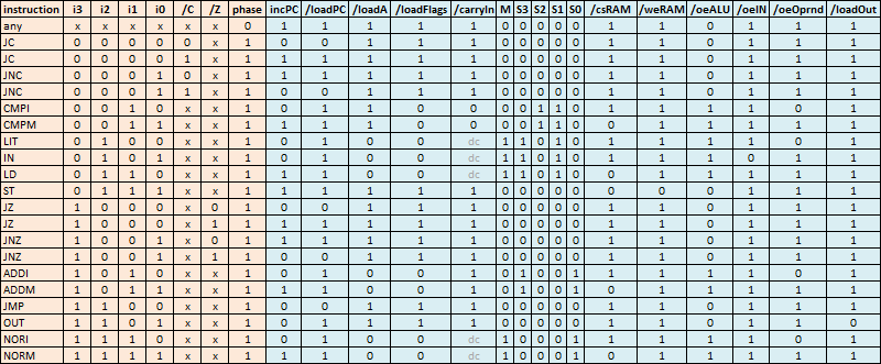
The first line of the table shows that phase 0 is the same for all instructions. That’s good, because at this point the instruction hasn’t been fetched from memory yet, so the CPU doesn’t even know what instruction it’s executing! The microcode drives the contents of the accumulator onto the data bus, even though they’re not needed – CMOS chips can exhibit problems if the bus is left to float. Also during phase 0, hardware loads the Fetch register with the program ROM byte, and the microcode advances the program counter to the next byte.
Phase 1 is where all the interesting work happens. ADDI is a good example of a typical instruction. Its instruction opcode is 1010 binary, or $A hex. For this instruction, the same control signals will be asserted regardless of the C or Z flags. /oeOprnd will be 0, enabling the bus driver to drive the immediate operand value onto the data bus, where it connects to one of the ALU inputs. The other ALU input is always connected to the accumulator register. The /carryIn, M, and S[0..3] control signals will be set to put the ALU into addition mode, with no carry-in. /loadA will be 0, so the ALU result will be stored to the accumulator. /loadFlags will also be 0, so the carry and zero flags will be updated with the results from the addition.
JZ (jump if zero) is another good example. Its instruction opcode is 1000 binary, or $8 hex. If the Z flag is 0 (meaning true), then incPC will be 0 (PC will not be incremented) and /loadPC will be 0 (PC will be loaded with the new address). So if Z is 0, the jump will be taken. If the Z flag is 1 (meaning false), then incPC will be 1 (PC will be incremented) and /loadPC will be 1 (PC will not be loaded). So if the Z flag is 1, the CPU just skips over the destination address byte and advances to the next instruction, without taking the jump. Jump instructions don’t need to involve the ALU, but they drive the accumulator value onto the data bus, so the bus won’t be left floating.
Note that some ALU control signals are irrelevant for certain instructions, and are shown in gray and labeled “dc” for don’t care.
Instruction Set
With only 4 bits for the instruction opcode, there’s a maximum of 16 different instructions, so the choice of which instructions to implement is challenging. It would be possible to have more than 16 instructions, but only by shrinking the address size or immediate operand size. Since this is a 4-bit CPU, a 4-bit instruction size just makes sense.
There are five types of jump instructions:
JMP – unconditional jump
JC – jump if carry
JNC – jump if no carry
JZ – jump if zero
JNZ – jump if not zero
This is a good set of jump instructions for convenient programming. Although they’re convenient, the negative jumps JNC and JNZ aren’t absolutely necessary, because you can always rewrite them with a positive jump and an unconditional jump:
JNC noCarry
carry:
   do stuff
noCarry:
   do other stuff
becomes
JC carry
JMP noCarry
carry:
   do stuff
noCarry:
   do other stuff
LD and ST load a nibble from data space (RAM) to the accumulator, or store a nibble from the accumulator to data space.
LIT loads a literal immediate nibble value to the accumulator. It might also have been named LDI.
OUT stores a nibble from the accumulator to one of the sixteen output ports, while IN loads a nibble from one of the sixteen input ports to the accumulator. These instructions are intended to be used for I/O.
ADDI adds a literal immediate nibble value to the accumulator, while ADDM adds a nibble in data space to the accumulator. In either case, the carry-in for the addition is 0, and the carry-out and zero flags are set by the results of the addition.
CMPI compares a literal immediate nibble value to the accumulator (subtracts the value from the accumulator), while CMPM compares a nibble in data space to the accumulator. The accumulator value is not modified, but the carry-out and zero flags are set by the results of the subtraction. Because the ALU is performing a subtraction, the carry-in is always 1 in order to make the math work out correctly.
NORI performs a NOR with an immediate value, NORM performs a NOR with a data space value. The carry-out and zero flags are set by the results of the NOR.
Synthetic Instructions
What about the instructions that aren’t here, like subtraction, AND, OR, NOT? Happily, all of these can be synthesized from the existing instructions. The assembler I’ve written includes some of these as macros, so they can be used as if they were built-in instructions.
NOT: NORI #0
ORI x: NORI x; NORI #0
ORM x: NORM x; NORI #0
ANDI x: NORI #0; NORI ~x
SUBI: ADDI (~x+1)
The only common instructions that can’t be trivially synthesized are ANDM and SUBM, because they require the use of a temporary register to hold the complement of the data space value. A dedicated location in data space could be used for this purpose, since Nibbler only has one register.
In many cases, with some thought you can eliminate the need for these synthetic instructions entirely. Take the common case of checking a specific bit in an input. On a CPU with an ANDI instruction, this might look like:
#define BIT2 $4 ; $4 = 0100
IN #0 ; load accumulator with nibble from port 0
ANDI BIT2
JNZ bit2is1
With Nibbler, you might think to rewrite this using the synthetic ANDI mentioned above:
#define NOT_BIT2 $B ; $B = 1011
IN #0 ; load accumulator with nibble from port 0
NORI #0
NORI NOT_BIT2
JNZ bit2is1
But this can be shortened by simplifying the two negatives NORI and JNZ into a single positive JZ:
#define NOT_BIT2 $B ; $B = 1011
IN #0 ; load accumulator with nibble from port 0
NORI NOT_BIT2
JZ bit2is1
Software Tools
I created several software tools to help make Nibbler development easier. Most were written in .NET languages like C#, using the free Visual Studio Express IDE for Windows.
Microcode Builder
The simplest tool is the Microcode Builder, which generates two binary files for the contents of the two microcode ROMs. In the beginning I intended to describe the microcode operations in a text file, using register transfer language, and then the Microcode Builder would assemble it into binary. But when it became clear the microcode would be fairly simple, I dropped the idea of using RTL, and just wrote some C code to generate the required binary data directly. The program contains lots of bit-shifting fun like:
    // 9 JNZ
    for (int c = 0; c < 2; c++)
    {
        microcode[(9 << 3) | (c << 2) | (0 << 1) | 1] = 0xF03F; // Z
        microcode[(9 << 3) | (c << 2) | (1 << 1) | 1] = 0x303F; // NZ
    }
Those hexadecimal numbers are just rows from the microcode table, with the 16 control signals expressed as a 4-nibble hex value.
Assembler
The Nibbler assembler is used to write programs for the CPU, using symbolic instruction names and branch labels. It was originally written for my Tiny CPU project, then adapted for Nibbler’s purposes. The assembler runs as a command line program. It takes a single .asm file as input, and assembles the code into a .bin binary output file. It also generates a .sym symbol file, containing the values of all the labels and constants in the code, as well as the assembled address of each line of code. The symbol file is used later by the simulator, in order to perform source-level debugging.
The assembler doesn’t have any fancy features like macros or conditional compilation, but it does support:
- Decimal constants
- Hex constants, preceded by $
- Character constants, contained in ‘ ‘ single quotes
- < and > operators to extract the high or low nibble of a byte constant
- Named constants using #define (both data and address constants)
- Named labels, and jumping to a named label
- Unnamed + and – labels, for jumping forward and backward
- Comments, starting with ;
For a good example of the kind of code the assembler can handle, look at the source for my guess the number program (old version).
Simulator
The most complex tool is the machine simulator. Originally developed for BMOW 1, this GUI-based tool simulates the data and control paths of the CPU. It supports source level symbolic debugging, disassembly, microcode debugging, code breakpoints, data breakpoints, memory inspection, and I/O simulation of the LCD and input buttons.
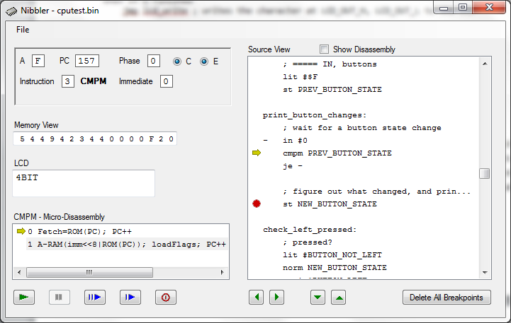
The simulator uses the program binary, the program source and symbol files (if available), and the microcode ROM binaries. In the image above, the simulator is doing source level debugging of a button watcher example program.
Execution is currently stopped at the CMPM PREV_BUTTON_STATE instruction, as shown by the yellow arrow. There’s a breakpoint two instructions further down, at the line with the red circle. If the simulator is started and a simulated button is pressed, the program will break out of the loop and stop at the breakpoint. (The JE instruction in the image was later replaced by JZ.)
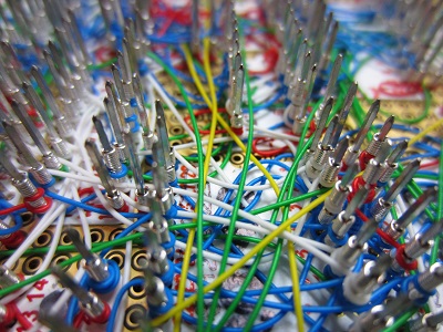
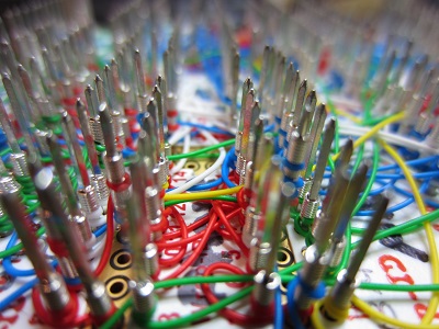
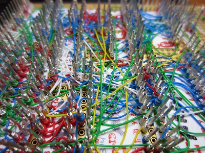
Photos
Recommend
About Joyk
Aggregate valuable and interesting links.
Joyk means Joy of geeK