

The transparent chip inside a vintage Hewlett-Packard floppy drive
source link: https://www.righto.com/2023/12/HP-silicon-on-sapphire-phi-chip.html
Go to the source link to view the article. You can view the picture content, updated content and better typesetting reading experience. If the link is broken, please click the button below to view the snapshot at that time.
Computer history, restoring vintage computers, IC reverse engineering, and whatever
The transparent chip inside a vintage Hewlett-Packard floppy drive
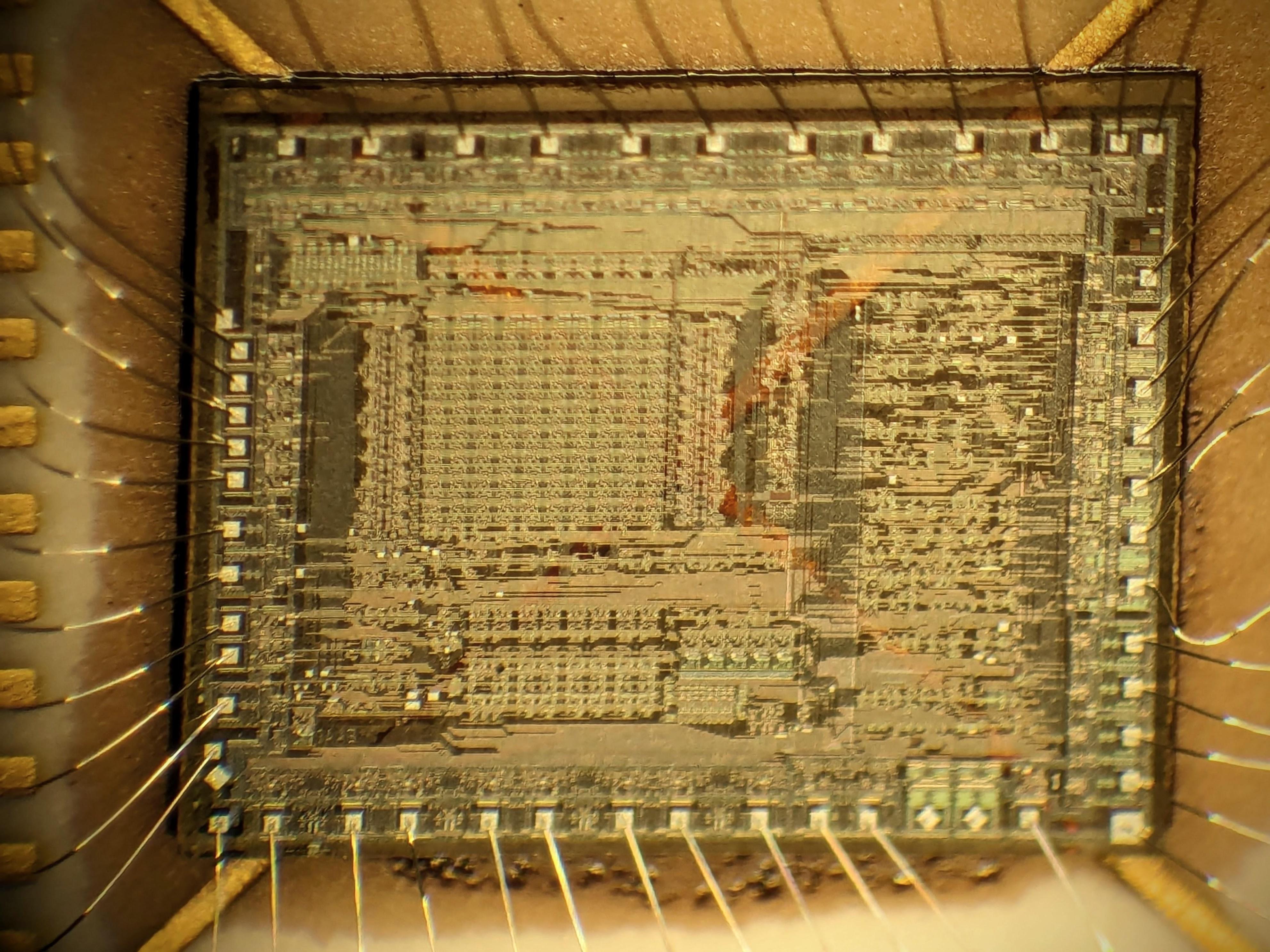
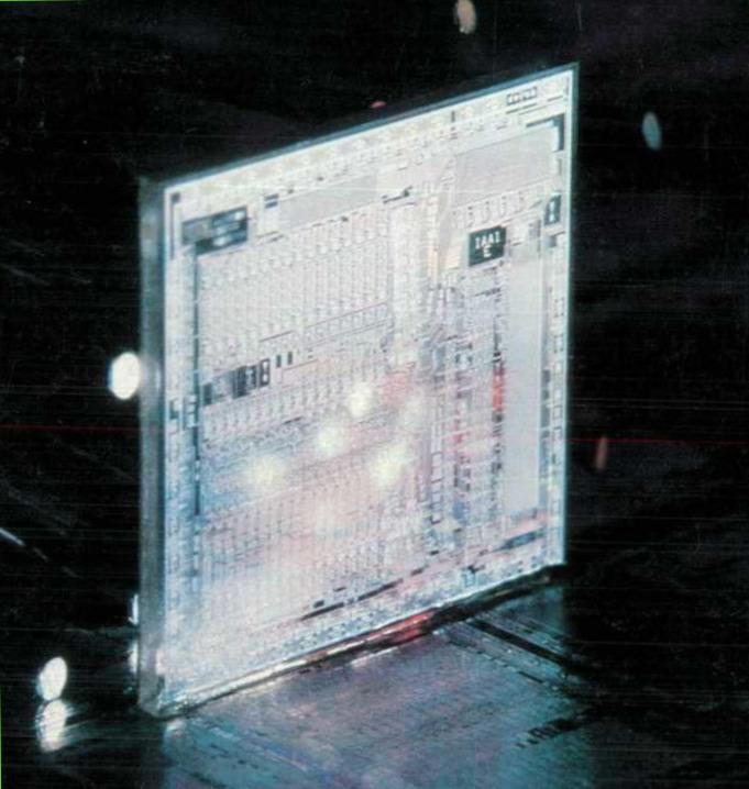
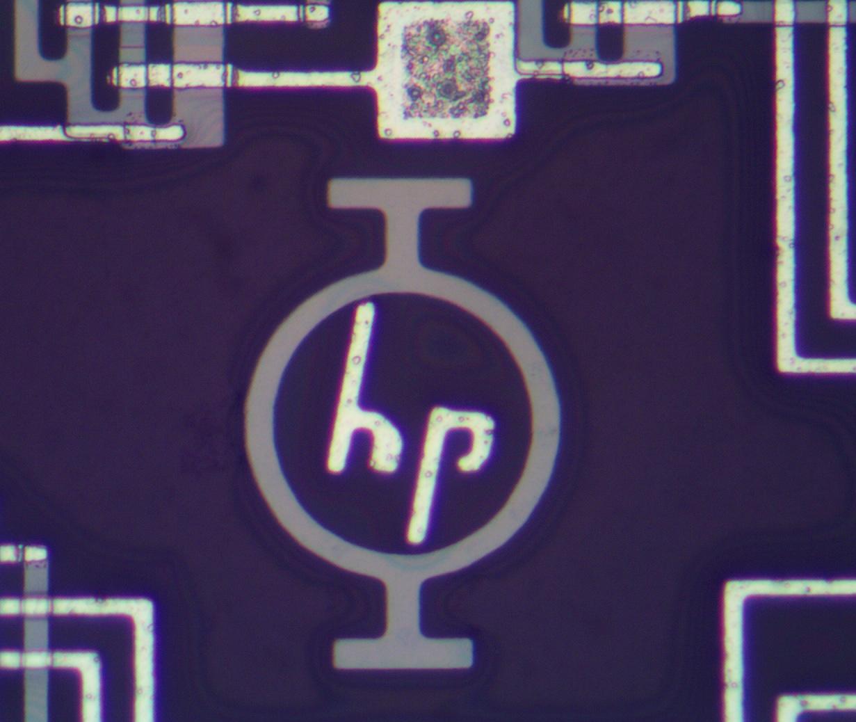
While repairing an eight-inch HP floppy drive, we found that the problem was a broken interface chip. Since the chip was bad, I decapped it and took photos. This chip is very unusual: instead of a silicon substrate, the chip is formed on a base of sapphire, with silicon and metal wiring on top. As a result, the chip is transparent as you can see from the gold "X" visible through the die in the photo below.
The chip is a custom HP chip from 1977 that provides an interface between HP's interface bus (HP-IB) and the Z80 processor in the floppy drive controller. HP designed this interface bus as a low-cost bus to connect test equipment, computers, and peripherals. The chip, named PHI (Processor-to-HP-IB Interface), was used in multiple HP products. It handles the bus protocol and buffered data between the interface bus and a device's microprocessor.1 In this article, I'll take a look inside this "silicon-on-sapphire" chip, examine its metal-gate CMOS circuitry, and explain how it works.
Silicon-on-sapphire
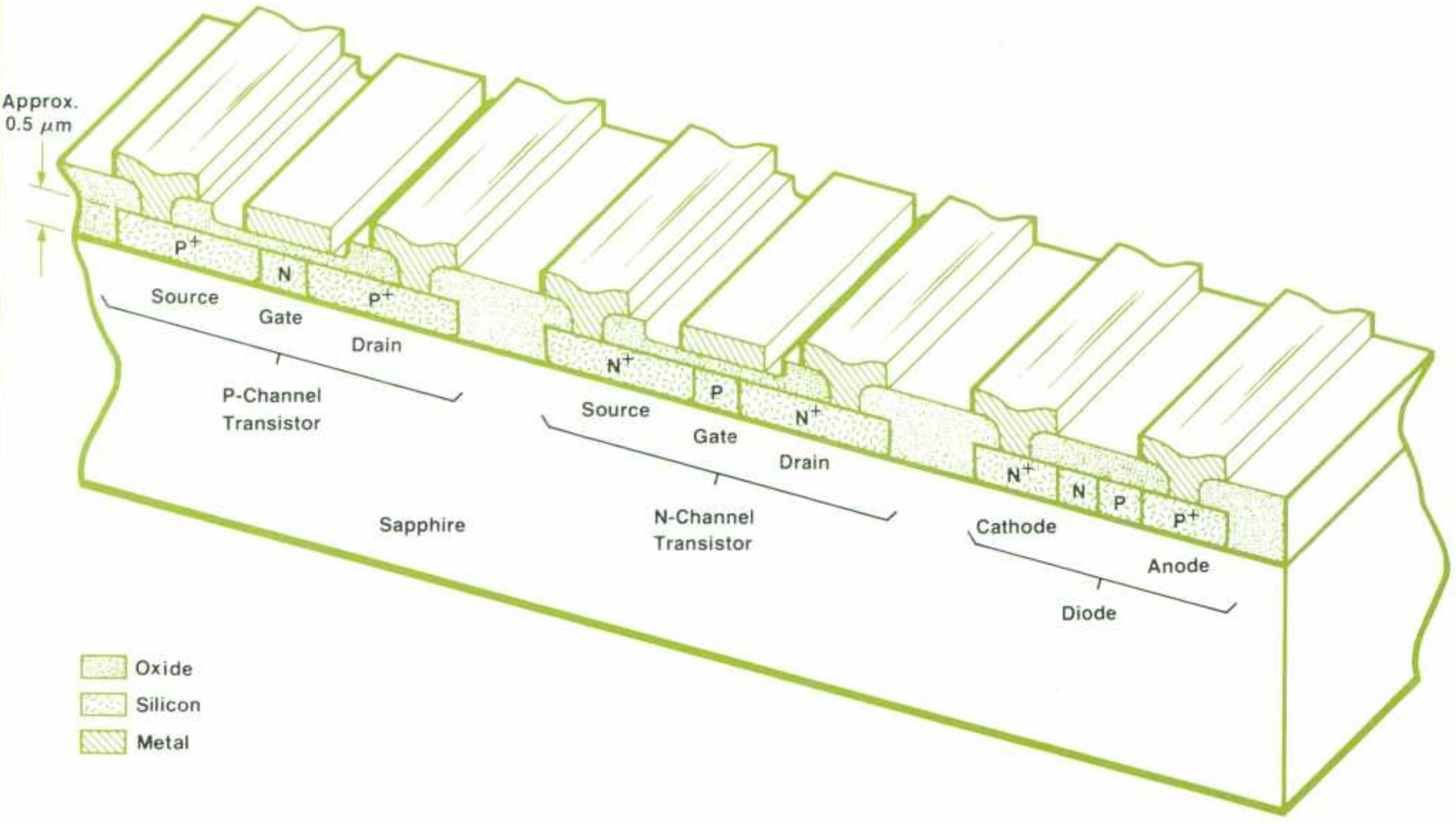
Most integrated circuits are formed on a silicon wafer. Silicon-on-sapphire, on the other hand, starts with a sapphire substrate. A thin layer of silicon is built up on the sapphire substrate to form the circuitry. The silicon is N-type, and is converted to P-type where needed by ion implantation. A metal wiring layer is created on top, forming the wiring as well as the metal-gate transistors. The diagram below shows a cross-section of the circuitry.
The important thing about silicon-on-sapphire is that silicon regions are separated from each other. Since the sapphire substrate is an insulator, transistors are completely isolated, unlike a regular integrated circuit. This reduces the capacitance between transistors, improving performance. The insulation also prevents stray currents, protecting against latch-up and radiation. Because of its resistance to radiation, silicon-on-sapphire found use in space applications.
Silicon-on-sapphire integrated circuits date back to research in 1963 at Autonetics, an innovative but now-forgotten avionics company that produced guidance computers for the Minuteman ICBMs, among other things. RCA developed silicon-on-sapphire integrated circuits in the 1960s and the RCA 1802 processor was used on the Galileo spacecraft. HP used silicon-on-sapphire for multiple chips starting in 1977, such as the MC2 Micro-CPU Chip. HP also used SOS for the three-chip CPU in the HP 3000 Amigo (1978), but the system was a commercial failure. The popularity of silicon-on-sapphire peaked in the early 1980s and HP moved to bulk silicon integrated circuits for calculators such as the HP-41C. Silicon-on-sapphire is still used in various products, such as LEDs and RF applications, but is now mostly a niche technology.
Inside the PHI chip
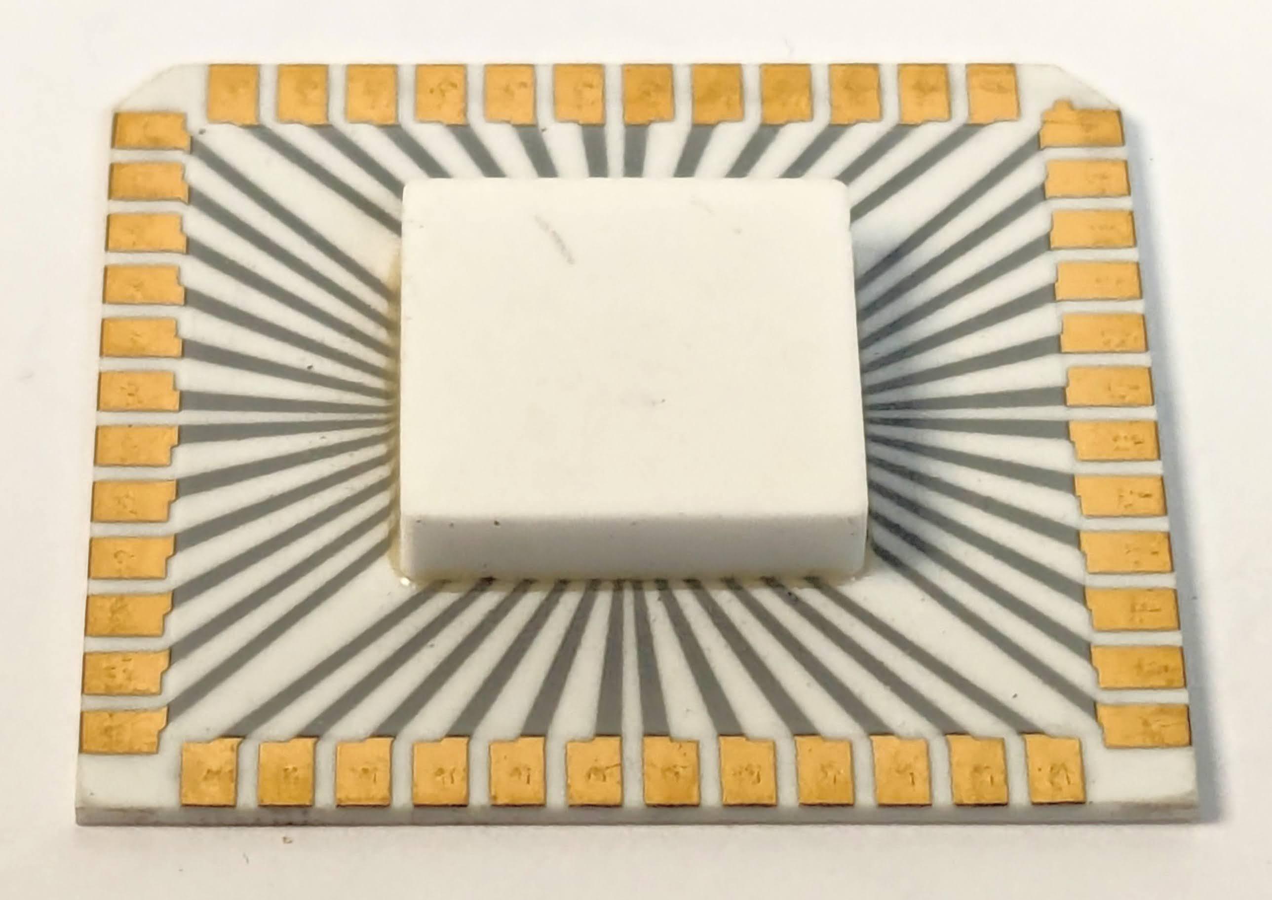
HP used an unusual package for the PHI chip. The chip is mounted on a ceramic substrate, protected by a ceramic cap. The package has 48 gold fingers that press into a socket. The chip is held into the socket by two metal spring clips.
Decapping the chip was straightforward, but more dramatic than I expected. The chip's cap is attached with adhesive, which can be softened by heating. Hot air wasn't sufficient, so we used a hot plate. Eric tested the adhesive by poking it with an X-Acto knife, causing the cap to suddenly fly off with a loud "pop" and sending the blade flying through the air. I was happy to be wearing safety glasses.
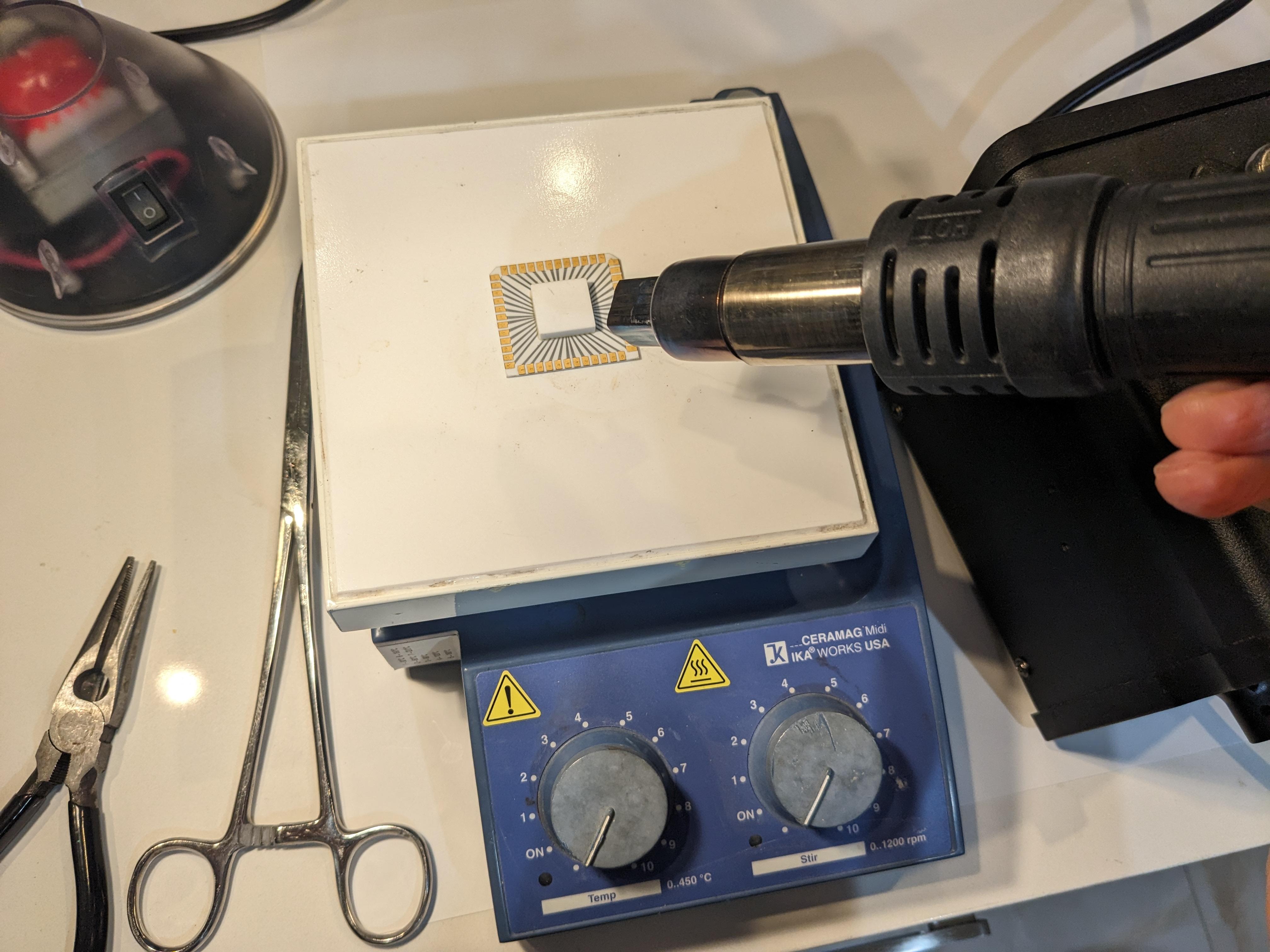
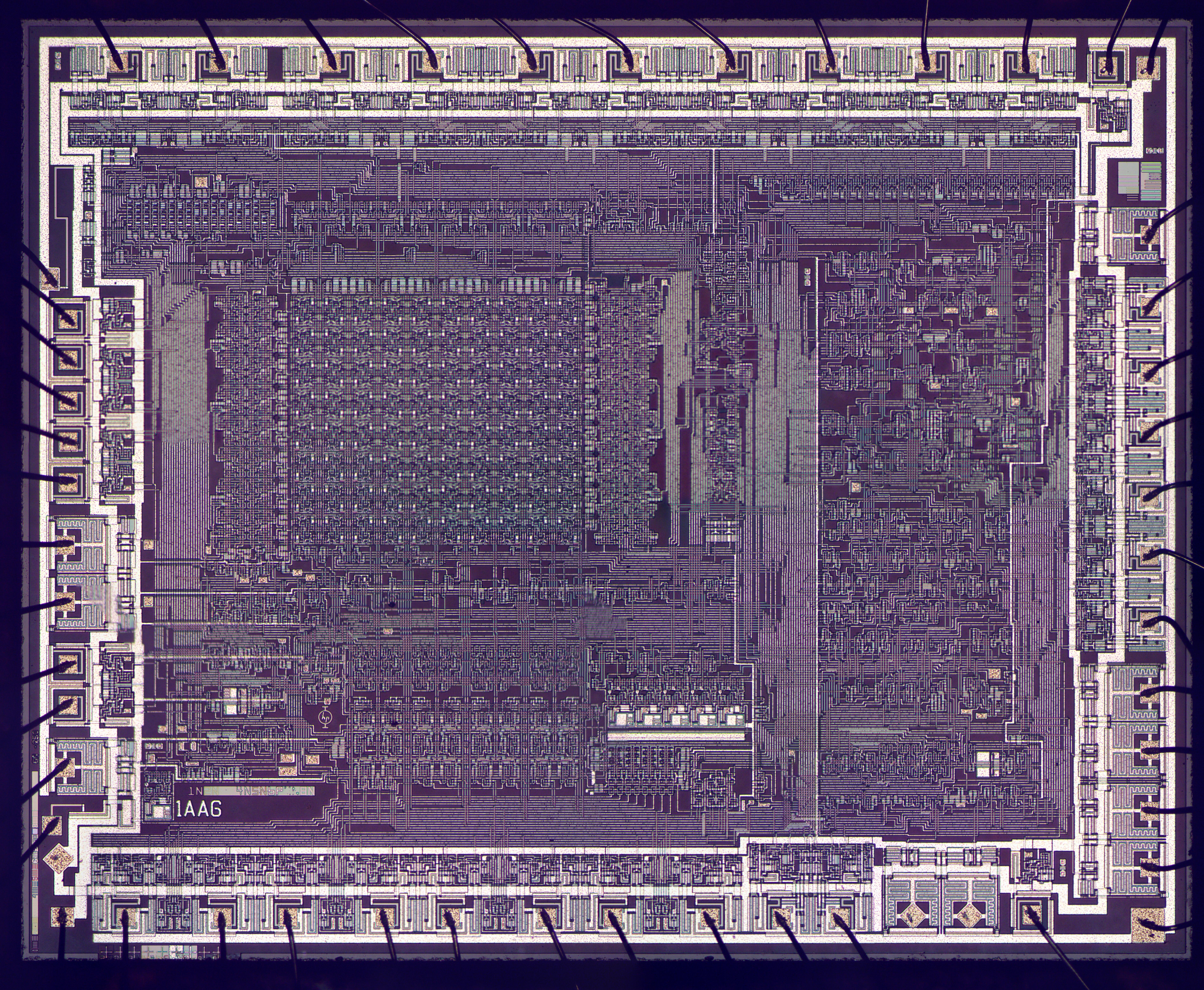
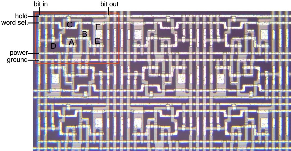
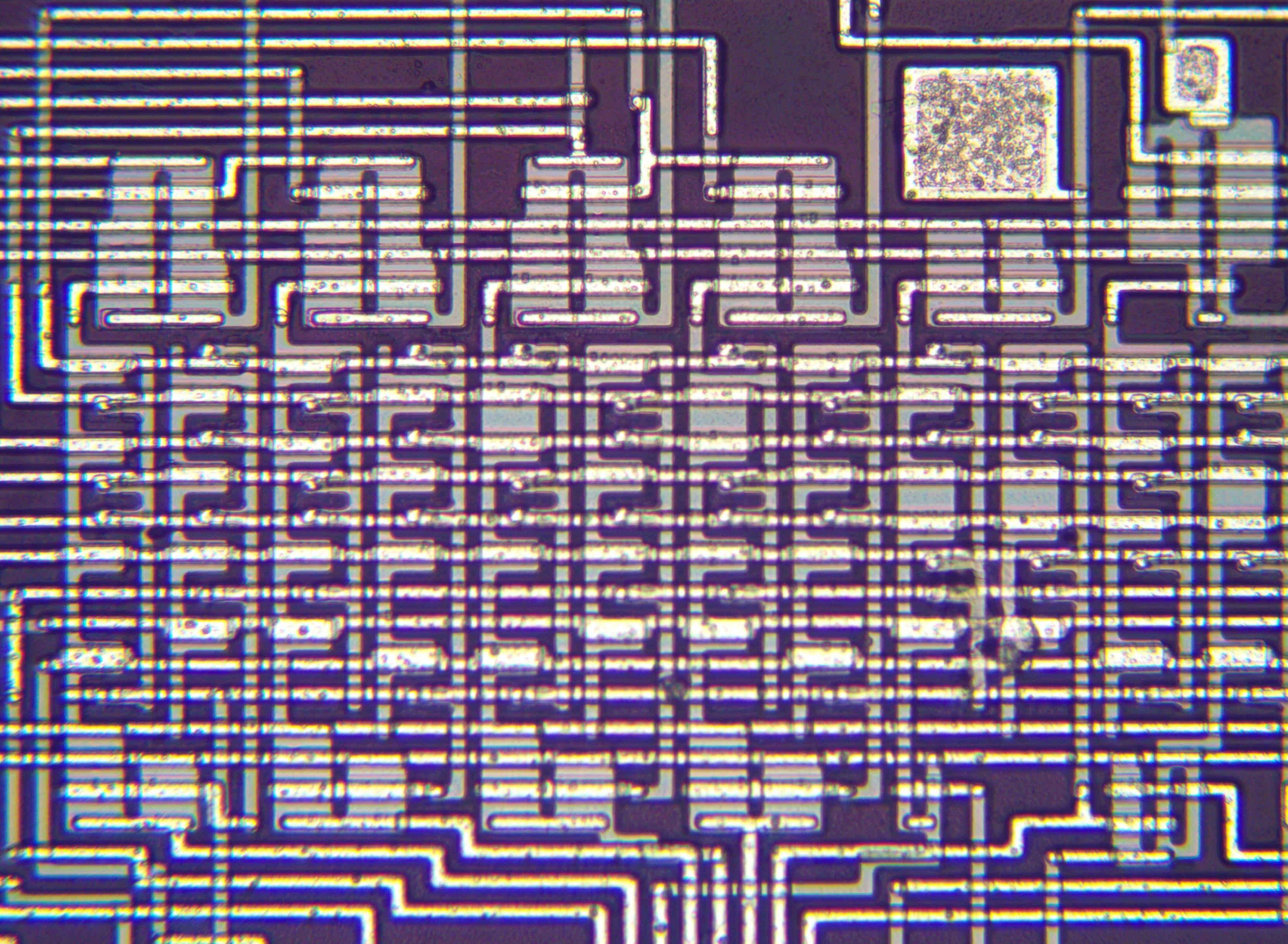
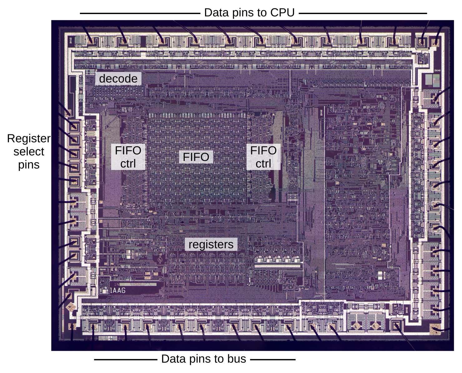
After decapping the chip, I created the high-resolution die photo below. The metal layer is clearly visible as white lines, while the silicon is grayish and the sapphire appears purple. Around the edge of the die, bond wires connect the chip's 48 external connections to the die. Slightly upper left of center, a large regular rectangular block of circuitry provides 160 bits of storage: this is two 8-word FIFO buffers, passing 10-bit words between the interface bus and a connected microprocessor. The thick metal traces around the edges provide +12 volts, +5 volts, and ground to the chip.
Logic gates
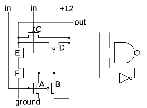
Circuitry on this chip has an unusual appearance due to the silicon-on-sapphire implementation as well as the use of metal-gate transistors, but fundamentally the circuits are standard CMOS. The photo below shows a block that implements an inverter and a NAND gate. The sapphire substrate appears as dark purple. On top of this, the thick gray lines are the silicon. The white metal on top connects the transistors. The metal can also form the gates of transistors when it crosses silicon (indicated by letters). Inconveniently, metal that contacts silicon, metal that crosses over silicon, and metal that forms a transistor all appear very similar in this chip. This makes it more difficult to determine the wiring.
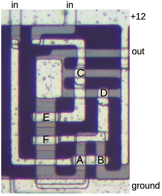
The schematic below shows how the gates are implemented, matching the photo above. The metal lines at the top and bottom provide the power and ground rails respectively. The inverter is formed from NMOS transistor A and PMOS transistor B; the output goes to transistors D and F. The NAND gate is formed by NMOS transistors E and F in conjunction with PMOS transistors C and C. The components of the NAND gate are joined at the square of metal, and then the output leaves through silicon on the right. Note that signals can only cross when one signal is in the silicon layer and one is in the metal layer. With only two wiring layers, signals in the PHI chip must often meander to avoid crossings, wasting a lot of space. (This wiring is much more constrained than typical chips of the 1970s that also had a polysilicon layer, providing three wiring layers in total.)
The FIFOs
The PHI chip has two first-in-first-out buffers (FIFOs) that occupy a substantial part of the die. Each FIFO holds 8 words of 10 bits, with one FIFO for data being read from the bus and the other for data written to the bus. These buffers help match the bus speed to the microprocessor speed, ensuring that data transmission is as fast as possible.
Each bit of the FIFO is essentially a static RAM cell, as shown below. Inverters A and B form a loop to hold a bit. Pass transistor C provides feedback so the inverter loop remains stable. To write a word, 10 bits are fed through vertical bit-in lines. A horizontal word write signal is activated to select the word to update. This disables transistor C and turns on transistor D, allowing the new bit to flow into the inverter loop. To read a word, a horizontal word read line is activated, turning on pass transistor F. This allows the bit in the cell to flow onto the vertical bit-out line, buffered by inverter E. The two FIFOs have separate lines so they can be read and written independently.
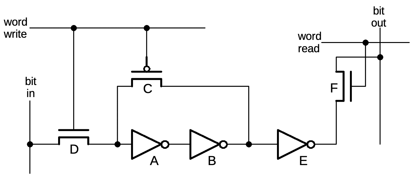
The diagram below shows nine FIFO cells as they appear on the die. The red box indicates one cell, with components labeled to match the schematic. Cells are mirrored vertically and horizontally to increase the layout density.
Control logic (not shown) to the left and right of the FIFOs manages the FIFOs. This logic generates the appropriate read and write signals so data is written to one end of the FIFO and read from the other end.
The address decoder
Another interesting circuit is the decoder that selects a particular register based on the address lines. The PHI chip has eight registers, selected by three address lines. The decoder takes the address lines and generates 16 control lines (more or less), one to read from each register, and one to write to each register.
The decoder has a regular matrix structure for efficient implementation. Row lines are in pairs, with a line for each address bit input and its complement. Each column corresponds to one output, with the transistors arranged so the column will be activated when given the appropriate inputs. At the top and bottom are inverters. These latch the incoming address bits, generate the complements, and buffer the outputs.
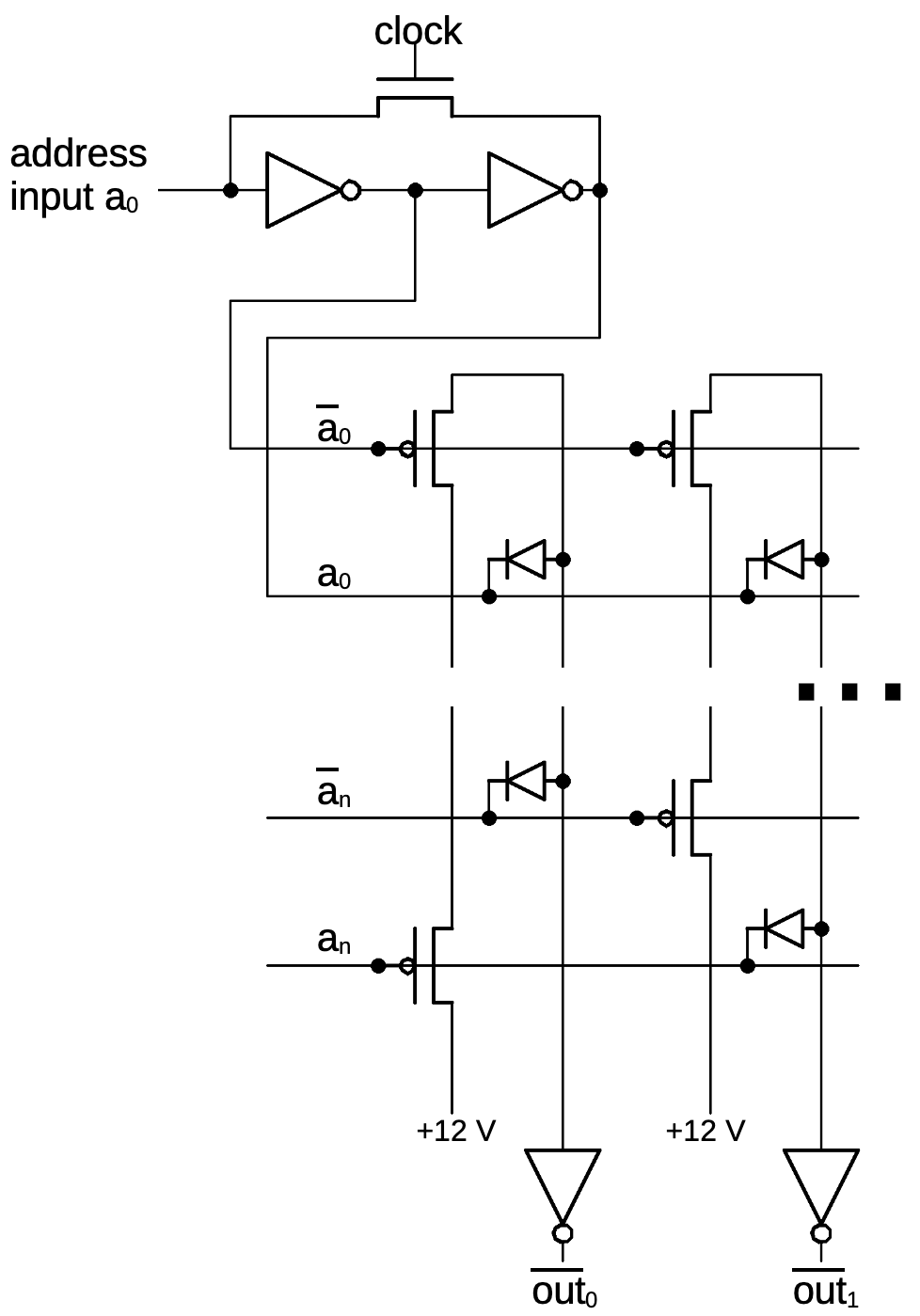
The schematic above shows how the decoder operates. (I've simplified it to two inputs and two outputs.) At the top, the address line goes through a latch formed from two inverters and a pass transistor. The address line and its complement form two row lines; the other row lines are similar. Each column has a transistor on one row line and a diode on the other, selecting the address for that column. For instance, supposed a0 is 1 and an is 0. This matches the first column since the transistor lines are low and the diode lines are high. The PMOS transistors in the column will all turn on, pulling the input to the inverter high. However, if any of the inputs are "wrong", the corresponding transistor will turn off, blocking the +12 volts. Moreover, the output will be pulled low through the corresponding diode. Thus, each column will be pulled high only if all the inputs match, and otherwise it will be pulled low. Each column output controls one of the chip's registers, allowing that register to be accessed.
The HP-IB bus and the PHI chip
The Hewlett-Packard Interface Bus (HP-IB) was designed in the early 1970s as a low-cost bus for connecting diverse devices including instrument systems (such as a digital voltmeter or frequency counter), storage, and computers. This bus became an IEEE standard in 1975, known as the IEEE-488 bus.2 The bus is 8-bits parallel, with handshaking between devices so slow devices can control the speed.
In 1977, HP Developed a chip, known as PHI (Processor to HP-IB Interface) to implement the bus protocol and provide a microprocessor interface. This chip not only simplified construction of a bus controller but also ensured that devices implemented the protocol consistently. The block diagram below shows the components of the PHI chip. It's not an especially complex chip, but it isn't trivial either. I estimate that it has several thousand transistors.
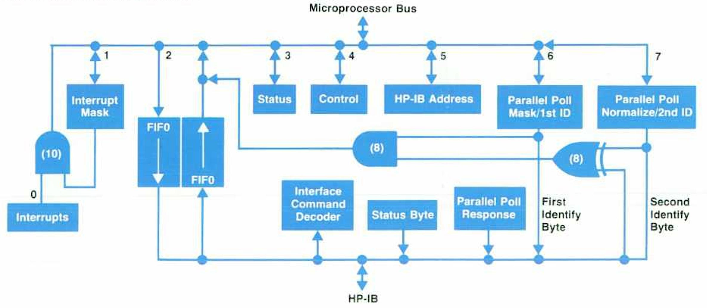
The die photo below shows some of the functional blocks of the PHI chip. The microprocessor connected to the top pins, while the interface bus connected to the lower pins.
Conclusions
The PHI chip is interesting as an example of a "technology of the future" that didn't quite pan out. HP put a lot of effort into silicon-on-sapphire chips, expecting that this would become an important technology: dense, fast, and low power. However, regular silicon chips turned out to be the winning technology and silicon-on-sapphire was relegated to niche markets.
Comparing HP's silicon-on-sapphire chips to regular silicon chips at the time shows some advantages and disadvantages. HP's MC2 16-bit processor (1977) used silicon-on-sapphire technology and had 10,000 transistors and ran at 8 megahertz, using 350 mW. In comparison, the Intel 8086 (1978) was also a 16-bit processor, but implemented on regular silicon and using NMOS instead of CMOS. The 8086 had 29,000 transistors, ran at 5 megahertz (at first) and used up to 2.5 watts. The sizes of the chips were almost identical: 34 mm2 for the HP processor and 33 mm2 for the Intel processor. This illustrates that CMOS uses much less power than NMOS, one of the reasons that CMOS is now the dominant technology. For the other factors, silicon-on-sapphire had a bit of a speed advantage but wasn't as dense. Silicon-on-sapphire's main problem was its low yield and high cost. Crystal incompatibilities between silicon and sapphire made manufacturing difficult; HP achieved a yield of 9%, meaning 91% of the dies failed.
The time period of the PHI chip is also interesting since interface buses were transitioning from straightforward buses to high-performance buses with complex protocols. Early buses could be implemented with simple integrated circuits, but as protocols became more complex, custom interface chips became necessary. (The MOS 6522 Versatile Interface Adapter chip (1977) is another example, used in many home computers of the 1980s.) But these interfaces were still simple enough that the interface chips didn't require microcontrollers, using simple state machines instead.
For more, follow me on Twitter @kenshirriff or RSS for updates. I'm also on Mastodon occasionally as @[email protected]. Thanks to CuriousMarc for providing the chip and to TubeTimeUS for help with decapping.
Notes and references
-
More information: The article What is Silicon-on-Sapphire discusses the history and construction. Details on the HP-IB bus are here. The HP 12009A HP-IB Interface Reference Manual has information on the PHI chip and the protocol. See also the PHI article from HP Journal, July 1989. EvilMonkeyDesignz also shows a decapped PHI chip. ↩
-
People with Commodore PET computers may recognize the IEEE-488 bus since peripherals such as floppy disk drives were connected using the IEEE-488 bus. The cables were generally expensive and harder to obtain than interface cables used by other computers. The devices were also slow compared to other computers, although I think this was due to the hardware, not the bus. ↩
Recommend
About Joyk
Aggregate valuable and interesting links.
Joyk means Joy of geeK