

Intel Downplays Hybrid CPU-GPU Engines, Merges NNP Into GPU
source link: https://www.nextplatform.com/2023/06/08/intel-downplays-hybrid-cpu-gpu-compute-engines-merges-nnp-into-gpu/
Go to the source link to view the article. You can view the picture content, updated content and better typesetting reading experience. If the link is broken, please click the button below to view the snapshot at that time.
Intel Downplays Hybrid CPU-GPU Engines, Merges NNP Into GPU
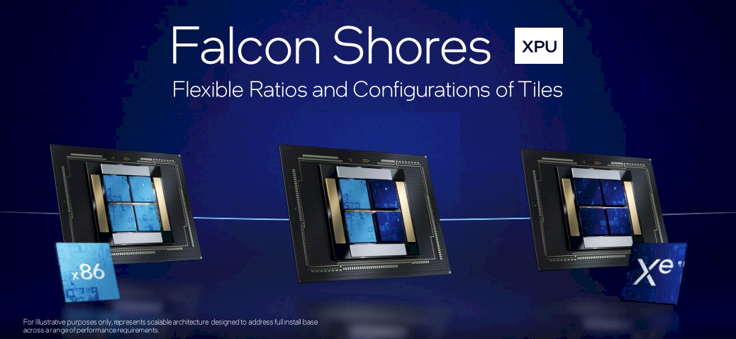
When Intel announced its “Falcon Shores” project to build a hybrid CPU-GPU compute engine back in February 2022 that allowed the independent scaling of CPU and GPU capacity within a single socket, it looked like the chip maker was preparing to take on rivals Nvidia and AMD head on with hybrid compute motors, which Intel calls XPUs, AMD calls APUs, and Nvidia doesn’t really have if you want to be strict about what its “superchips” are and what they are not.
As we pointed out at the time, this “Aurora in a socket” approach of putting a changeable mix of CPU and GPU chiplets into a Xeon SP socket with literally the same main memory and a very low latency link between the chiplets allows for more complex AI inference than the AMX matrix math unit in a Xeon SP could handle as well as more HPC floating point processing than is possible in an AVX-512 vector unit without making customers resort to a higher latency, discrete GPU in the Max Series line or indeed a discrete GPU from either Nvidia or AMD.
When announced by Raja Koduri, who was general manager of the Accelerated Computing Systems and Graphics business at Intel – which has been discontinued in the wake of Koduri leaving Intel in March of this year – Intel was promising that Falcon Shores would deliver more than 5X better performance per watt, more than 5X higher compute density in an X86 socket, and more than 5X higher memory bandwidth and capacity with what it called “extreme bandwidth shared memory.” We presume that these numbers were compared to an “Ice Lake” Xeon SP server socket, and both were top bin parts at that.
Falcon Shores was timed for 2024, and widely expected to plug directly into the same “Mountain Stream” server platform used by the future “Granite Rapids” Xeon SPs. And we conjectured that Intel could do something crazy, like give the GPU an emulation layer that made it look like a big, fat AVX-512 vector math unit to simplify programming. (Or more likely an AMX unit, now that we think on it a little bit more.)
By March of this year, as Koduri was leaving Intel, the company started back pedaling not only on offering what looked like five different CPU-GPU chiplet mixes inside of a Xeon SP socket, but also killed off the “Rialto Bridge” kicker to the “Ponte Vecchio” Max Series GPU that will be doing most of the 2 exaflops peak of processing in the “Aurora” supercomputer at Argonne National Laboratory. There were rumors at the time that the first Falcon Shores devices would come out in 2025, and only with GPU chiplets on them, making the device basically a discrete GPU replacement for Ponte Vecchio in lieu of Rialto Bridge. Rialto Bridge was flushed because Intel wanted to move to a two-year GPU cadence on its roadmaps – and reasonably so because that is what Nvidia and AMD are doing.
At the recent ISC23 supercomputing conference in Hamburg, Intel clarified its intentions with regard to Falcon Shores, confirming that not only that this device would be a GPU-only compute engine, but that the time for hybrid XPUs was not yet right.
“My prior push and emphasis around integrating CPU and GPU into an XPU was premature,” explained Jeff McVeigh, general manager of the Super Compute Group, in briefings for the ISC23 event. And frankly, McVeigh is probably taking responsibility for something that was really a decision made by Koduri and perhaps even with Jim Keller in the mix, who left to become chief executive officer and now chief technology officer of AI startup Tenstorrent more than two years ago.
“And the reason is,” McVeigh continued in his explanation, “we feel like we are in a much more dynamic market than we thought even just a year ago – all the innovation around generative AI large language models. While much of that has been in the commercial space, we see that being much more broadly adopted in scientific endeavors as well. And when you are in that dynamic market, where the workloads are changing rapidly, you really do not want to force yourself down a path of a fixed CPU to GPU ratio. You don’t want to fix the vendors or even the architectures used between X86 and Arm – which ones are the best ones for that allow for flexibility, allow for good software support across them – versus when you’re in a mature market. When the workloads are fixed, when you have really good clarity of them, that they’re not going to be changing dramatically, integration is great. We have done integration many, many times. It helps with cost, it drives down power. But you are fixed. You are fixed with the suppliers for those two components, you are fixed with how they’re configured. And we just feel like our real reckoning with where the market is today that it’s not time to integrate.”
Given that Nvidia is set to sell a pretty high number of “Grace” CPU and “Hopper” GPU superchips and AMD has at least one big customer (Lawrence Livermore National Laboratory) buying lots of its “Antares” Instinct MI300A hybrid CPU-GPU compute engines, we are certain that Nvidia and AMD would utterly disagree with this assessment.
Maybe such XPU integration is not right for Intel, which has to slash costs and focus on making money in its core server CPU market like it has not had to focus since the Itanium debacle from the late 1990s and early 2000s. Or even more precisely, maybe not for Intel CPU cores and Intel GPU cores. Perhaps Intel CPU cores and Nvidia GPU cores would be more palatable to the market? Up until now, Nvidia did not have a server CPU business, so perhaps the time has passed for that potential partnership, which might have seen NVLink ports added to “Sapphire Rapids” and a giant HBM3 complex.
In any event, this is not the first time that Intel has contemplated a “frankenchip” design with auxiliary compute outside of the X86 cores in its Xeon server chips. And this is also not the first time it pulled back on those efforts.
Intel divulged that a hybrid CPU-FPGA device was under development back in June 2014, and was showing off a hybrid 15-core Broadwell-Arria 10 GX prototype at the Open Compute Summit back in March 2016. In May 2018, when the hybrid CPU-FPGA product was formally launched, the CPU side was upgraded to a 20-core Skylake chiplet and the Arria 10 GX was the FPGA side of the package. Intel has, of course, sold Intel Xeon E3 processors with CPUs and GPUs on a single die for many, many years, but rarely talks about the latent – and not just inexpensive but essentially free – floating point math capabilities inherent in that integrated GPU. (We frequently remind people of this, like we did here.) Intel stopped talking about the hybrid CPU-FPGA design many years ago, and never talked about its low-end CPU-GPU possibilities, much less how it might do something like the originally conceived Falcon Shores slated for 2024 alongside the Granite Rapids Xeon SPs.
Now, the Falcon Shores multi-chip GPU is slated for 2025, paired with the “Clearwater Forest” Xeon SP kicker to Granite Rapids.
Speaking of frankenchips, McVeigh said something very interesting in his roadmap presentation at the ISC23 briefing. First, the roadmap:
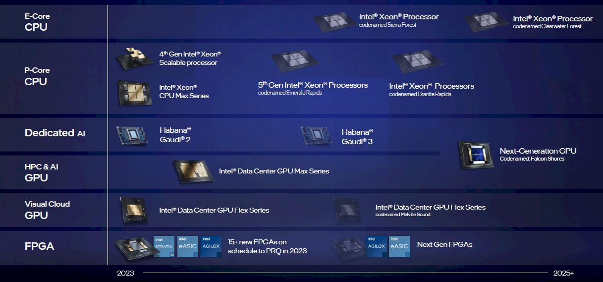
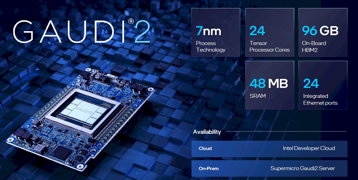
Since May 2022, Intel has been shipping the Gaudi2 matrix math engines that came from its $2 billion acquisition of Habana Labs in December 2019. And the Gaudi3 follow-on, which we know almost nothing about and which taped out in March of this year, looks like it is coming in early 2024.
After that and at the point where the Falcon Shores multi-chip GPU hits the roadmap in 2025, the line separating Gaudi from the Ponte Vecchio and Falcon Shores GPUs disappears. If you have an NNP with massive amounts of mixed precision matrix math and a GPU with massive amounts of mixed precision matrix math, maybe you don’t need a Gaudi4 if you can count on a Falcon Shores that might have equivalent oomph. Especially if you need to pare down slash costs like Intel does to reach its goals of cutting $3 billion in costs in 2023 and cutting another $5 billion to $7 billion in costs across 2024 and 2025 inclusive.
McVeigh said that Falcon Shores would be aimed at both HPC and AI workloads, be upgraded to HBM3 memory, and would “bring together the best from our Gaudi products, which includes standard Ethernet switching” and “I/O designed for scale.”
That I/O looks like it will be CXL over PCI-Express linking the CPUs to the Falcon Shores GPUs, but will use an enhanced version of the Ethernet fabric created by Habana Labs to mesh the GPUs together, if we read this correctly. (We are perplexed as to why this won’t all be PCI-Express 6.0 switching, but then again, that will be limited to a few racks due to PCI-Express cable lengths and the relatively low number of ports on PCI-Express.)
The Gaudi1 chip could scale to 128 devices interlinked with this Ethernet fabric running RoCE. Each Gaudi1 had ten 100 Gb/sec Ethernet ports, and you could put either four devices or eight devices in a node and scale to either 32 nodes or 16 nodes to reach 128 fully interconnected nodes. The Gaudi2 device scales to 24 integrated Ethernet ports running at 100 Gb/sec, which connect eight devices to each other in an all-to-all, non-blocking topology:
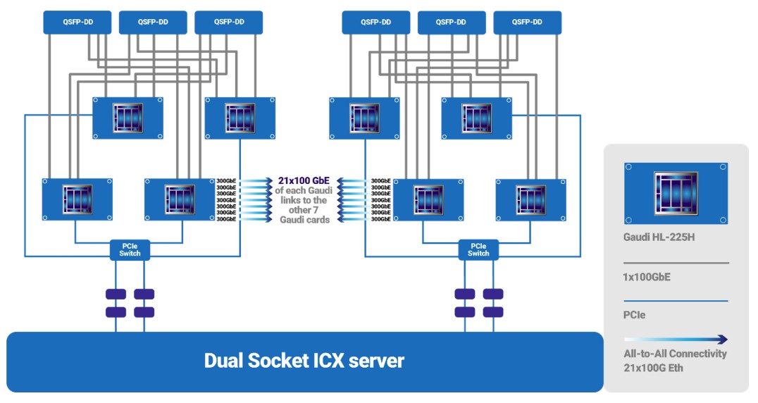
To create the eight-way Gaudi2 system, 21 of the 24 ports on each device are used to make that all-to-all link between the matrix engines. Three ports from each device are aggregated in a staggered fashion to a total of six QSFP-DD ports coming out of the Gaudi2 chassis, providing the interconnect to scale across 16 or 32 Gaudi enclosures, which as we said, is done with regular Ethernet switches.
It is not hard to imagine this Gaudi Ethernet fabric being upgraded to 400 Gb/sec or maybe even 800 Gb/sec ports coming off the Falcon Shores GPU and using similarly fast Ethernet switches to link even more devices together. More the pity that Intel no longer has an Ethernet switching business, since it has mothballed its Tofino line from its Barefoot Networks acquisition. Customers will have to choose Ethernet switching based on Broadcom, Nvidia, Marvell, or Cisco Systems silicon.
It also looks like Intel is going to be taking the systolic arrays – what we call matrix math engines – from the Gaudi device and using them instead of the Xe matrix math engines used on the Ponte Vecchio design. So, yeah, don’t be counting on Gaudi 4 being a distinct product.
So much for that $2.35 billion experiment in NNPs that came from the acquisitions of Nervana Systems and Habana Labs. The future NNP is a GPU at Intel. And the only companies that will buy Gaudi2 and Gaudi3 are those who are desperate for any matrix math capabilities and who also are committed to Intel’s future Falcon Shores GPUs.
Sign up to our Newsletter
Featuring highlights, analysis, and stories from the week directly from us to your inbox with nothing in between.
Subscribe now
Recommend
About Joyk
Aggregate valuable and interesting links.
Joyk means Joy of geeK