

Second IC :)
source link: http://sam.zeloof.xyz/second-ic/
Go to the source link to view the article. You can view the picture content, updated content and better typesetting reading experience. If the link is broken, please click the button below to view the snapshot at that time.

Second IC :)
Homemade 1000+ transistor array chip
In 2018 I made the first homemade integrated circuits in my garage fab. I was a senior in high school when I made the Z1 amplifier, and now I’m a senior in college so there are some long overdue improvements to the amateur silicon process.
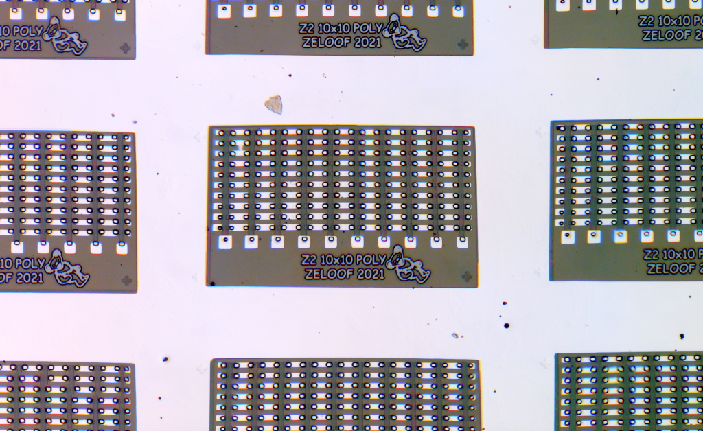
The Z1 had 6 transistors and was a great test chip to develop all the processes and equipment. The Z2 has 100 transistors on a 10µm polysilicon gate process – same technology as Intel’s first processor. My chip is a simple 10×10 array of transistors to test, characterize, and tweak the process but this is a huge step closer to more advanced DIY computer chips. The Intel 4004 has 2,200 transistors and I’ve now made 1,200 on the same piece of silicon.
Previously, I made chips with a metal gate process. The aluminum gate has a large work function difference with the silicon channel beneath it which results in a high threshold voltage (>10V). I used these metal gate transistors in a few fun projects like a guitar distortion pedal and a ring oscillator LED blinker but both of these required one or two 9V batteries to run the circuit due to high Vth. By switching to a polysilicon gate process, I get a ton of performance benefits (self aligned gate means lower overlap capacitances) including a much lower Vth which makes these chips compatible with 2.5V and 3.3V logic levels. The new FETs have excellent characteristics:
NMOS Electrical Properties:
Vth             = 1.1 V
Vgs MAX         = 8 V
Cgs             = <0.9 pF
Rise/fall time  = <10 ns
On/off ratio    = 5.2e4
Leakage current = 59 nA (25°C)
I was particularly surprised by the super low leakage current. This value goes up about 10x in ambient room lighting.
Now we know that it’s possible to make really good transistors with impure chemicals, no cleanroom, and homemade equipment. Of course, yield and process repeatability are diminished. I’ll do more testing to collect data on the statistics and variability of FET properties but it’s looking good!
The chip is small, about one quarter the die area of my previous ICs (2.4mm^2) which makes it hard to probe. There’s a simple 10×10 array of N-channel FETs on each chip which will give me a lot of characterization data. Since it’s such a simple design, I was able to lay it out using Photoshop. Columns of 10 transistors share a common gate connection and each row is strung together in series with adjacent transistors sharing a source/drain terminal. It’s similar to NAND flash but I only did this to keep the metal pads large enough so I can reasonably probe them, if every FET had 3 pads for itself they would be too small.
A single 10µm NMOS transistor can be see below, with slight misalignment in the metal layer (part of the left contact is uncovered). Red outline is polycrystalline silicon, blue is the source/drain.
So far I’ve made an opamp (Z1) and a memory-like array (Z2). More interesting circuits are definitely possible even with this low transistor density. The process needs some tweaking but now that I’m able to consistently make good quality transistors I should be able to design more complex digital and analog circuits. Testing each chip is very tedious so I am trying to automate the process and I’ll post more data then. I’ve made 15 chips (1,500 transistors) and know there’s at least one completely functional chip and at least two “mostly functional”, meaning ~80% of the transistors work instead of 100%. No proper yield data yet. The most common defect is a drain or source shorted to the bulk silicon channel, not a leaky or shorted gate like on my Z1 process.
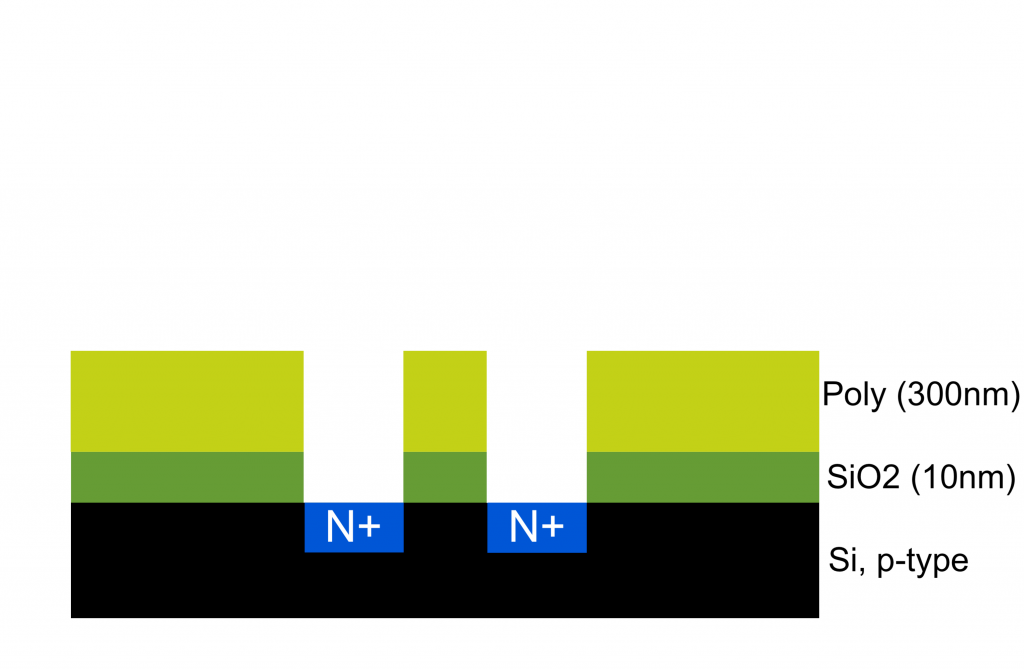
Profilometer scan of gate layer (y axis in angstrom, x axis is micron)I said before that the gate used to be made out of aluminum and now it’s silicon which makes the chips work a lot better. Silicon comes in three varieties that we care about: amorphous, polycrystalline, and monocrystalline. From left to right, these become more electrically conductive but also much harder to deposit. In fact, monocrystalline Si can’t be deposited, you can only grow it in contact with another mono-Si layer as a seed (epitaxy). Since the gate must be deposited on top of an insulating dielectric, poly is the best we can do. We can heavily dope the polysilicon anyway to make it more conductive.
A typical self-aligned polysilicon gate process requires Silane, a toxic and explosive gas, to deposit polycrystalline silicon layers. It may also be possible by sputtering or evaporating amorphous silicon and annealing with a laser. A major theme of this DIY silicon process is to circumvent expensive, difficult, or dangerous steps. So, I came up with a modified process flow. It’s a variation on the standard self-aligned methods to allow doping via high temperature diffusion rather than ion implantation. The effect is that I’m able to buy a silicon wafer with the polysilicon already deposited on it from the factory and pattern it to make transistors instead of putting my own polysilicon down halfway through the process. This is a nice short term workaround but it would be best to design a polysilicon deposition process using the laser anneal method mentioned above.
Wafers are available with all kinds of materials deposited on them already, so I just had to find one with a thin layer of SiO2 (gate oxide, ~10nm) followed by a thicker polysilicon (300nm). I found a lot of 25 200mm (EPI, prime, [1-0-0], p-type) wafers on eBay for $45 which is essentially a lifetime supply, so email me if you want one. The gate oxide is the most fragile layer and requires the most care during fabrication. Since I bought the wafer with a nice high quality oxide on it already that was capped off and kept clean by the thick polysilicon layer, I was able to eliminate all the aggressive cleaning chemicals (sulfuric acid, etc) from the process and still make great transistors. Minimal process chemicals and tools are listed below.
Chemicals used in home poly-gate process:
-Water
-Alcohol
-Acetone
-Phosphoric acid
-Photoresist
-Developer (2% KOH)
-N type dopant (filmtronics P509)
-HF (1%) or CF4/CHF3 RIE
-HNO3 for poly etch or SF6 RIE
Equipment used in home poly-gate process:
-Hotplate
-Tube furnace
-Lithography apparatus
-Microscope
-Vacuum chamber to deposit metal
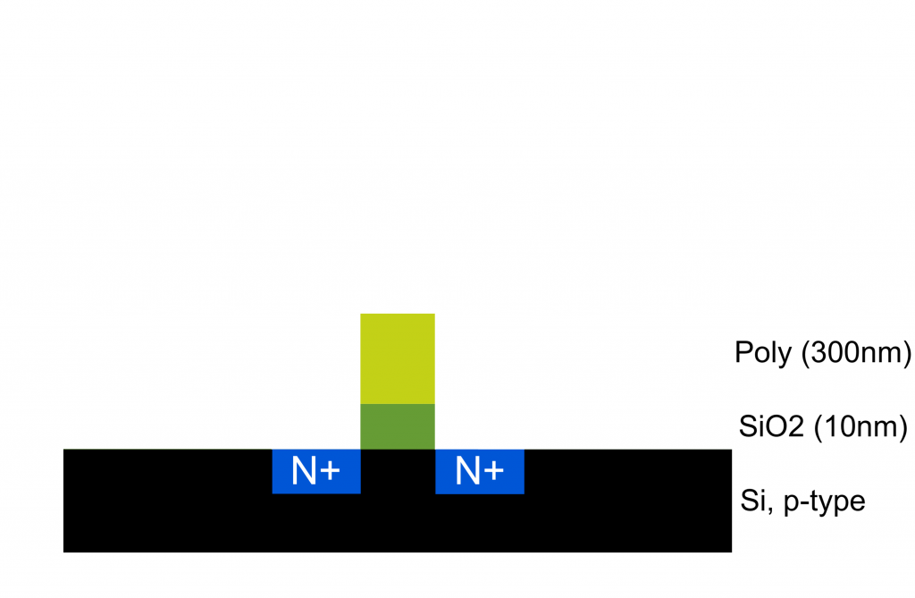
Z2 “gate first” process:


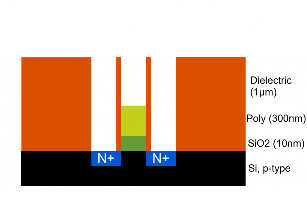

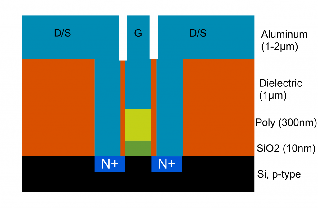
This process isn’t ideal and I want to make some changes so it’s CMOS compatible but it simplifies fabrication and makes it possible with a minimal set of tools. The 1µm dielectric layer (orange) would ideally be CVD SiO2 (it’s possible to build a TEOS oxide reactor at home) but I used a photoresist instead. Most photoresists can be baked around 250°C to form a hard permanent dielectric layer that is an easy alternative to CVD or PECVD oxide. A spin-on-glass/sol-gel could also be used here.
Huge composite stitched die image:
Thanks for following my work and feel free to contact me with your thoughts at [email protected] !
Recommend
About Joyk
Aggregate valuable and interesting links.
Joyk means Joy of geeK