

No space wasted: Embedding capacitors into interposers to increase miniaturizati...
source link: https://techxplore.com/news/2021-06-space-embedding-capacitors-interposers-miniaturization.html
Go to the source link to view the article. You can view the picture content, updated content and better typesetting reading experience. If the link is broken, please click the button below to view the snapshot at that time.

June 1, 2021
No space wasted: Embedding capacitors into interposers to increase miniaturization
by Tokyo Institute of Technology
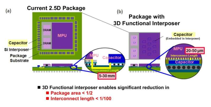 The new interposer design with an embedded capacitor provides a notable reduction in area requirements and interconnect length, leading to lower wiring resistance and parasitic capacitance. MPU: Microprocessing unit; DRAM: Direct random-access memory. Credit: The 2021 IEEE Electronic Components and Technology Conference
Scientists at Tokyo Institute of Technology develop a 3D functional interposer—the interface between a chip and the package substrate—containing an embedded capacitor. This compact design saves a lot of package area and greatly reduces the wiring length between the chip's terminals and the capacitor, allowing for less noise and power consumption. Their approach paves the way to new semiconductor package structures with greater miniaturization.
Electronics started big size-wise but have only grown smaller and more compact over time. Today, even smartphones outperform the bulky computers from the 1980s by orders of magnitude. Unfortunately, this accelerating trend in performance and scale is bound to slow down considerably as the materials and designs we use approach their physical limits. To overcome such problems, it is critical to think out of the box and come up with designs that address technological bottlenecks.
Over the last decade, progress in an essential passive component in electronics, the capacitor, has stagnated in some regards. Although we can fabricate much smaller capacitors than ever before, their actual capacity per unit area hasn't been improving as much. We need ways to make capacitors occupy less space while preserving their performance.
But what if we could integrate capacitors inside another element commonly used in modern circuits: the interposer? At Tokyo Institute of Technology, Japan, a team of scientists led by Professor Takayuki Ohba have committed to developing technologies to sustain the scaling of semiconductor circuits. In their latest study, which will be presented at the Proceedings of the 2021 IEEE Electronic Components and Technology Conference, they demonstrated that silicon interposers—the planar interface that holds and vertically connects an integrated chip with a circuit package or another chip—can be made into functional capacitors, thus saving up considerable space, and bringing along a ton of benefits.
In modern '2.5D' packages, chips such as DRAMs and microprocessors sit atop interposers with through-silicon vias, vertical conducting tunnels that bridge the connections in the chips with solder bumps on the package substrate. Capacitors are placed on the package substrate close to the components they serve, and a connection between their terminals and those of the chip has to be made, spanning 5-30 mm. This layout not only increases the necessary package substrate area, but also causes problems such as high wiring resistance and noise due to the long interconnections.
In stark contrast with this design, the team at Tokyo Tech cut the middleman and directly made the interposer be the silicon capacitor. They achieved this through a novel fabrication process in which the capacitive elements are embedded inside a 300 mm silicon piece using permanent adhesive and mold resin. The interconnects between the chip and the capacitor are made directly with through-silicon vias and without the need for solder bumps. "Our bumpless 3D functional interposer enables a notable reduction in package area of about 50% and an interconnect length a hundred times shorter," remarks Ohba.
The researchers also managed to cleverly avoid the two most common problems of bumpless chip-on-wafer designs, namely warping in the wafer due to the resin and misplacement errors due to void pockets in the adhesive. Through testing and theoretical calculations, they determined their functional interposer allowed for a wiring resistance about a hundred times lower than conventional designs, as well as a lower parasitic capacitance. These features could enable the use of lower supply voltages, leading to lower power consumption. "The chip-on-wafer integration technology we are developing will open up new routes in the evolution of semiconductor package structures," concludes Ohba excitedly. Overall, this study is a perfect example of the creative leaps that are needed if the accelerating march of technology is to be maintained.
Explore further
Recommend
-
126
The Linux Scheduler: a Decade of Wasted Cores - Lozi et al. 2016 This is the first in a series of papers from EuroSys 2016. There are three strands here: first of all, there's some great background into how scheduling works in the Linux kernel;...
-
108
Post with 1517 votes and 1019077 views. Shared by donthitsave. Don't Hit Save - Wasted Time
-
45
Rough IMHO as of 2019-02-05 There are far too many distributions and desktop environments. So much time and effort goes into developing, establishing, hosting, updating, maintaining, advertising Linux di...
-
12
High Code Coverage is not Wasted Effort Jan 8, 2018 • Tim MyerscoughTags: quality
-
6
The UK Has Wasted 50 Years Fighting a Losing War on DrugsOn the 50th anniversary of the Misuse of Drugs Act, VICE World News analysis shows just how catastrophically it has failed.May 26, 2021,...
-
5
Andrei F. on Twitter: "@blu51899890 I'm looking at this and wondering how easy he makes that black gunk removal look, and also thinking to myself HOW ISN'T HE BLOWING AWAY THOSE TWO CAPACITORS. I've messed that part up so many times."Don’t...
-
7
September 21, 2021
-
6
Notes on capacitors, part 1: ceramics & MLCCs I’ve been reading about capacitors a lot lately. Not just their high-level circuit behaviours, but also their materials and physical properties. I put together a hea...
-
4
Notes on capacitors, part 2: aluminium electrolytics This is part two of my “convert a bunch of notes I made about capacitors into a blog post” series. If you missed part one, which covered ceramics and MLCCs, y...
About Joyk
Aggregate valuable and interesting links.
Joyk means Joy of geeK