

Reverse-engineering a vintage comparator chip
source link: http://www.righto.com/2021/04/reverse-engineering-vintage-comparator.html
Go to the source link to view the article. You can view the picture content, updated content and better typesetting reading experience. If the link is broken, please click the button below to view the snapshot at that time.

Reverse-engineering a vintage comparator chip
I recently saw an interesting die photo of an unknown chip on Twitter, so I did some analysis of it. Looking at the circuitry inside, the chip appears to be four comparators, probably in the ECL (Emitter Coupled Logic) family. This is a quick blog post to summarize my investigation.
The die photo below shows the chip under the microscope. Regions of the silicon appear pink, blue, or yellow, depending on how the silicon was doped. The speckled regions are the metal layer on top of the silicon, wiring the circuitry together. Around the edges, the black bond wires connect the chip to the external pins. These wires are attached to the square bond pads. The die has four blocks of circuitry, one for each of its four comparators. Much of the die is unused, especially the large metal area in the middle. Because this chip's circuitry is relatively simple, it only uses a fraction of the available space.

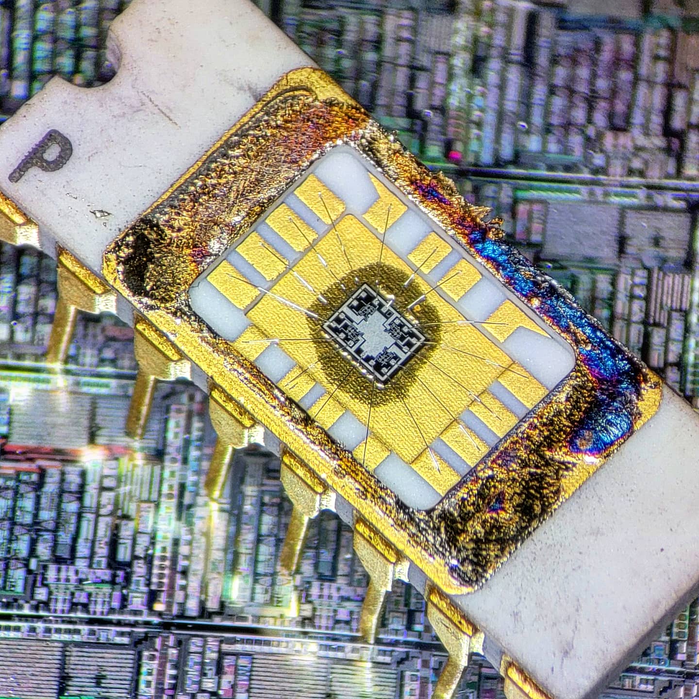
The photo below shows the chip with its metal lid removed. Modern chips are usually in a black epoxy package, but this chip has a white ceramic package. The tiny silicon die is visible in the middle, with bond wires connecting the die to the lead frame, the metal connections to the chip's gold-plated pins. The metal layer on top of the die is visible, and can be matched with the die photo above. The semi-circular notch on the left indicates the orientation of the chip; the "P" is pin 1.
The chip's components
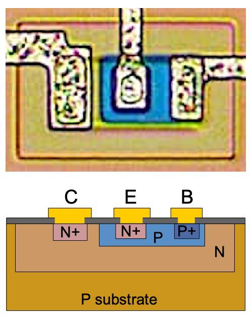
Transistors are the key components in a chip. This chip uses a type of transistor called the NPN transistor. The photo below shows a transistor as it appears on the chip. The orange and blue colors are regions of silicon that have been doped differently, forming N and P regions. The speckled areas are the metal layer of the chip on top of the silicon—these form the wires connecting to the transistor's collector, emitter, and base.
Underneath the photo is a cross-section drawing showing approximately how the transistor is constructed. There's a lot more than just the N-P-N sandwich you see in books, but if you look carefully at the vertical cross-section below the 'E', you can find the N-P-N that forms the transistor. The emitter (E) wire is connected to N+ silicon. Below that is a P layer connected to the base contact (B). And below that is an N+ layer connected (indirectly) to the collector (C). The emitter, base, and collector can be distinguished on the die with careful examination. The base's region surrounds the emitter, forming a blue rectangle. The collector contact is larger and off to the side.
The other key components of this chip are the resistors. The photo below shows two resistors as they appear on the die. The resistors are formed from strips of higher-resistance P silicon, which appears blue in the die photos. The two ends of each resistor are connected to the metal layer. A resistor has higher resistance if it is longer and narrower. While one resistor below is a simple rectangle, the other has a complex zig-zag shape to fit more length into the available space. (The blue rectangle in the lower right is a transistor, not a resistor. To distinguish it from a resistor, note that it has three contacts, and the two contacts on the rectangle are not symmetrical.)
The circuitry
Once the components can be recognized on the die, the circuit can be traced out and reverse-engineered. But before I describe the complete circuit, I'll explain one important functional block.
The schematic below shows a differential pair, or long-tailed pair, which amplifies the difference between its two inputs. This circuit is common in analog circuits, forming the heart of an op-amp. It is also the basis of Emitter-Coupled Logic (ECL). The basic idea is that a current sink (the two circles at the bottom) generates a fixed current I. This current gets split between the left path (I1) and the right path (I2). If the transistor on the left has a higher input voltage than the transistor on the right, most of the current will go to the left. But if the transistor on the right has a higher input, most of the current will go to the right. This circuit amplifies the voltage difference: even a small difference between the two inputs will switch most of the current from one side to the other.
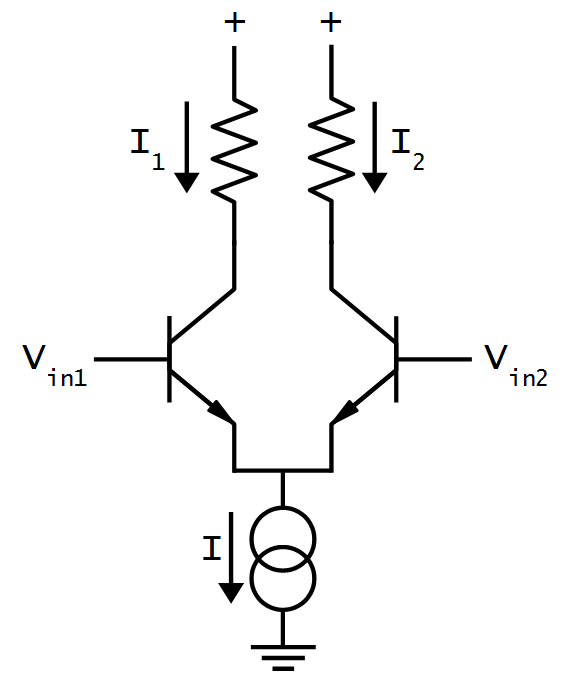
In this chip, the circuit is used as a comparator, a circuit that compares the two inputs and generates a logic output that indicates which input is higher. The side with the current will get pulled low, while the other side is pulled high by the resistor. Thus, the output can be treated as a logic signal.
The schematic below shows the circuitry for one of the four comparators on the chip. Note that the differential amplifier circuit above is used twice. For better performance, the output from the first differential amplifier is fed into a second differential amplifier. This sharpens the output: if the inputs are close together, the outputs from the first stage may not be fully "0" or "1". The second stage amplifies this difference, providing solid "0" and "1" outputs. The current sinks provide a relatively constant current for the amplifiers, but I won't explain them in detail.
The diagram below shows the circuitry on the die, corresponding to the schematic above. The red boxes indicate the transistors for the two amplifier stages and their associated current sinks. The other components are the resistors, which appear as blue rectangles. The wiring in the metal layer connects the components together, as well as the inputs on the left and the output at the top.
The diagram below shows how the circuitry of the chip maps onto its 16 pins. Each triangle represents a comparator with its positive and negative inputs. Two of the comparators have a single output, while two also have an inverted output (indicated by a bubble).
Conclusion
So what is this chip? Maybe it's simply four comparators, but they could have a specific purpose. The chip could be a converter for four differential input signals, e.g. DCS (Differential Current Switch) logic. Another chip in the family seems to be Emitter-Coupled Logic, so this chip could be four ECL inverters (but it doesn't make sense to have four pins for the reference voltage). It's a bit puzzling that two comparators have inverted and noninverted outputs, while two have single outputs.
Based on the circuitry and ceramic packaging of this chip, I estimate that it is from around 1970. The chip is labeled "OQ104", so I did a bunch of searching through old databooks, but I couldn't find anything that matches it. Since the chip looks like ECL and has the part number 104, it's tempting to think that the chip might be the 10,104 part in the MECL 10,000 series. Unfortunately, the 10,104 is a quad AND gate, and the internal circuitry is different. The "P" on the chip might indicate Philips, but I couldn't find any matching Philips components. For now, the exact identity of this chip is a mystery.
I announce my latest blog posts on Twitter, so follow me @kenshirriff. Many thanks to EvilMonkeyz Designs for providing the photos; follow on Instagram or Twitter for more interesting die photos.
Recommend
-
5
Ken Shirriff's blog Computer history, restoring vintage computers, IC reverse engineering, and whatever
-
8
die photos and reverse engineering Inside the 74181 ALU chip: die photos and reverse engineering What's inside a TTL chip? To find out, I opened up a 74181 ALU chip, took high-resolution die photos, and reverse-engineered the chi...
-
8
Reverse-engineering an early calculator chip with four-phase logic Reverse-engineering an early calculator chip with four-phase logic In 1969, high-density MOS integrated circuits were still new and logic circuits were construc...
-
6
reverse-engineering the vintage MC14500B A one-bit processor explained: reverse-engineering the vintage MC14500B The Motorola MC14500B1...
-
5
Reverse-engineering the standard-cell logic inside a vintage IBM chip Reverse-engineering the standard-cell logic inside a vintage IBM chip Integrated circuits are often built from standard-cell logic, constructed from standardi...
-
7
Ken Shirriff's blog Computer history, restoring vintage computers, IC reverse engineering, and whatever
-
9
Reverse-engineering a vintage power supply chip from die photos Reverse-engineering a vintage power supply chip from die photos I recently did a PC power...
-
5
Reverse-engineering the Yamaha DX7 synthesizer's sound chip from die photos Reverse-engineering the Yamaha DX7 synthesizer's sound chip from die photos The Yamaha DX7 digital synthesizer was released in 1983 and became "one of t...
-
11
Ken Shirriff's blog Computer history, restoring vintage computers, IC reverse engineering, and whatever ...
-
7
Ken Shirriff's blog Computer history, restoring vintage computers, IC reverse engineering, and whatever ...
About Joyk
Aggregate valuable and interesting links.
Joyk means Joy of geeK