

Investigating a failure to read DIMM SPD data on Intel Xeon Scalable platforms –...
source link: https://codeinsecurity.wordpress.com/2021/04/17/investigating-a-failure-to-read-dimm-spd-data-on-intel-xeon-scalable-platforms/
Go to the source link to view the article. You can view the picture content, updated content and better typesetting reading experience. If the link is broken, please click the button below to view the snapshot at that time.

Investigating a failure to read DIMM SPD data on Intel Xeon Scalable platforms
Memory DIMMs have a small flash memory chip (EEPROM) on them, containing an important descriptor table called the Serial Presence Detect (SPD). This data tells the system the size, speed, timings, operating voltage, manufacturer, part number, overclocking profiles, and all sorts of other information about each DIMM. The SPD chip is accessed using the SMBus protocol, which is based on I2C.
Tools such as CPU-Z, RAMMon, and RW Everything can be used to read the SPD data by talking to the flash chip over a hardware SMBus interface, using a driver. In many modern Intel systems the SMBus access is performed via the Platform Controller Hub (PCH), also known as the chipset. The problem is that none of these tools work properly on my system.

I’m running a C620 series chipset with a pair of Xeon Scalable 2nd generation processors, which is somewhat unusual, so it’s not entirely surprising that the tools are struggling. That being said, the SMBus interface on the Intel PCH has been standardised for quite a while, so there must be something a little different going on.
I ran RAMMon with logging enabled and contacted PassMark to report the bug. They asked if either Temperature Sense On DIMM (TSOD) or Closed Loop Thermal Throttling (CLTT) were enabled in the BIOS, since the two features apparently have caused issues in the past. I couldn’t see options for them, so I grabbed a BIOS update package and extracted the contents to see if I could figure out if either of these features were configured.
I threw the update into uefi-firmware-parser, with the following command:
python2 /usr/local/bin/uefi-firmware-parser -e -O --superbrute WS-C621E-SAGE-ASUS-6201.CAPThis extracted all the firmware components, including individual EFI binaries, into a subdirectory. I then ran strings over every file, so that I could search for anything related to TSOD or CLTT.
find ./ -type f -exec bash -c 'strings -t x -a $1 > $1.strings && strings -t x -a -e l $1 >> $1.strings && strings -t x -a -e b $1 >> $1.strings' find-sh {} \;This runs strings three times over each binary, once for 7-bit ASCII strings, then again for little- and big-endian UTF-16 string, since strings will only look for one string type per execution. The -a flag tells strings to look through the entire file, and -t x tells it to prefix each string with its hexadecimal offset in the file.
I got some hits very quickly. One of the EFI binaries in the BIOS, with a GUID of 6b6fd380-2c55-42c6-98bf-cbbc5a9aa666, had the following strings:
  9a1a2 Throttling Mode
  9a1c3 Configure Thermal Throttling Mode.
  9a20a OLTT
  9a215 CLTT
  9a220 CLTT with PECI
Loading the EFI PE into CFF Explorer allowed me to see where these offsets sat in the file.

The offsets of the strings are around 0x9a200, which is firmly inside the resource section. The resource directory parser and resource editor did not really give me much more than a giant blob of strings, though, so that didn’t help much.
My next idea was to just load the EFI PE into Ghidra. As standard, Ghidra isn’t great at EFI-specific stuff, so it’s helpful to have some extensions. The first one I used was the UEFI helper script in ghidra-firmware-utils, which found a bunch of the GUIDs and other bits for me. I also tried to install efiSeek, but ran into problems with the compilation. Instead, I grabbed the Behemotx64.gdt types archive from the repo and loaded that in, allowing me to have access to common EFI structure definitions.
I got a little way through reverse engineering this binary, but it didn’t do me much good. EFI strings are stored in a kind of string table that’s accessed by index, making it impossible for Ghidra to automatically identify references. Even after parsing the string table with a custom script that labelled the entries by index, it turns out that most of the user interface stuff is itself defined through a whole heap of metadata and bytecode. It’s probably possible to turn this back into something readable, but it’s just too much effort.
The next thing I thought to do was just look at the CPU datasheet. Intel has fairly good technical datasheets for their CPUs and PCHs. For the CPUs they’re usually split into two volumes, the first containing electrical specs and the second containing registers. Searching for TSOD in there turned out to be a quick win – one of the first hits was in relation to a register called smb_stat_[0:1]. It turns out that each of the two Integrated Memory Controllers (IMCs) on the CPU has a dedicated SMBus interface built in.
In order to check whether this interface was being used, I launched RAMMon with the DEBUGMODE flag. This dumped a lot of detailed logs out, including information about the discovery, enumeration, and attempts to access SMBus and SPD devices. It showed the following results:
11.297s - SysInfo:  Found SMBus device:  VID:8086 DID:A1A3 Bus:00 Dev:1F Fun:04 IO Add:0780 IO (2) Add:0000 MMIO Add:0000000000000000 PCI Add:{00:00:00:0000} Rev:09 [Intel C620 Series Chipset Family SMBus]

11.313s - SysInfo:  Found SMBus device:  VID:8086 DID:2085 Bus:17 Dev:1E Fun:05 IO Add:0000 IO (2) Add:0000 MMIO Add:0000000000000000 PCI Add:{17:1E:05:0000} Rev:05 [Intel Skylake-X]

11.328s - SysInfo:  Found SMBus device:  VID:8086 DID:2085 Bus:85 Dev:1E Fun:05 IO Add:0000 IO (2) Add:0000 MMIO Add:0000000000000000 PCI Add:{85:1E:05:0000} Rev:05 [Intel Skylake-X]
This shows that three SMBus devices were detected:
- C620 PCH SMBus interface at bus 0x00, device 0x1F, function 0x04, with VID 0x8086 / DID 0xA1A3.
- Skylake-X CPU SMBus interface at bus 0x17, device 0x1E, function 0x05, with VID 0x8086 / DID 0x2085.
- Skylake-X CPU SMBus interface at bus 0x85, device 0x1E, function 0x05, with VID 0x8086 / DID 0x2085.
This makes sense, since I have a C620 series chipset and a pair of Skylake-X CPUs, but the device and function numbers for the CPU SMBus interfaces do not match the description of the IMC SMBus interfaces in the datasheet.
The IMC Registers are implemented in the following Bus, Device, Functions:
Bus: B(2), Device: 10, 12, Function: 0
Device 10 applies to IMC 0. Device 12 applies to IMC 1.– Intel Xeon Scalable 2nd Generation Datasheet (Vol. 2) – Section 3: Integrated Memory Controller (iMC) Configuration Registers (pg. 19)
The CPU SMBus interfaces that RAMMon detected are at device 0x1E, function 0x05, and there is only one per CPU. However, the IMC SMBus interfaces are at devices 10 (0x0A) and 0x12 (0x0C), function 0, and there are two of them per CPU since there are two IMCs per CPU. This means that RAMMon is either mis-detecting the SMBus interface on the CPU, or is using a different SMBus interface (it’s possible that there are multiple).
The datasheet describes the IMC SMBus interface as being dedicated to DIMM access. At this point, I started to realise the problem: all of the tools were attempting to use general-purpose SMBus interfaces to talk to the SPD chips on the DIMMs, but in Xeon Scalable platforms the memory has its own special dedicated SMBus interface.
Luckily, I had a copy of the Project Olympus motherboard schematics on hand. It’s a completely open hardware design for a modern dual-socket Intel Xeon Scalable platform server motherboard. Sure enough, the index showed that there was a section called CPU_DIMM_SMBUS on page 100.
Note: the OpenCompute wiki is really outdated and full of dead links; you can now find the design collateral files here.

The chips in the middle are NXP PCA9617A I2C bus repeaters. All they really do here is handle logic level translation between VCCIO voltage on the CPU and VPP voltage on the RAM, and keep bus capacitance to a minimum. For clarity, let’s take a closer look at the connections:
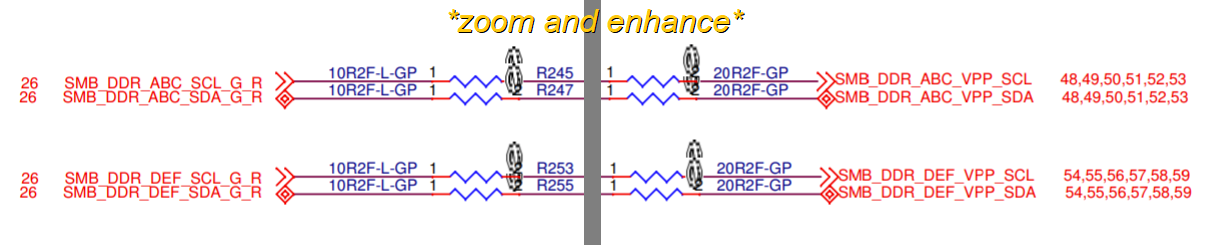
The connections on the left are marked SMB_DDR_xyz_SCL_G_R and SMB_DDR_xyz_SDA_G_R, for clock and data respectively, and on the right they’re marked as SMB_DDR_xyz_VPP_SCL_R and SMB_DDR_xyz_VPP_SDA_R to match. Searching for these terms shows the rest of the picture – the left side goes to the CPU socket, whereas the right goes to the DIMMs.
For fun, I also loaded up the board view file in Allegro Free Viewer (OpenBoardView doesn’t support this binary format, unfortunately) to find the physical locations of the chips on the board.

The fact that these parts’ pads are in red means that they’re actually on the rear side of the board, which is a shame because I couldn’t find a picture of the rear of a real board. Instead you’ll have to make do with this picture of the front of the board, with the component locations marked out.
Switching back to volume 1 of the datasheet, containing the electrical specifications, descriptions of the DDRxxx_SPDSCL and DDRxxx_SPDSDA signals can be found:
Signal NameDescriptionDDR{012,235}_SPDSCLSMBus clock for the dedicated interface to the serial presence detect (SPD) and thermal sensors (TSoD) on the DIMMs. DDR_SCL_C012 is used for memory channels 0, 1, and 2 while DDR_SCL_C345 is used for memory channels 3, 4, and 5.DDR{012,235}_SPDSDA SMBus data for the dedicated interface to the serial presence detect (SPD) and thermal sensors (TSoD) on the DIMMs. DDR_SDA_C012 is used for memory channels 0, 1, and 2 while DDR_SDA_C345 is used for memory channels 3, 4, and 5. Table 4-2: Memory Channel Miscellaneous, from page 56 of the Intel Xeon Scalable 2nd Generation Datasheet (Vol. 1)
This concretely confirms my suspicions – you can’t use the usual CPU SMBus interfaces that are shared with PCIe devices to talk to the DIMMs, nor can you use the PCH SMBus either. You need to go through the IMCs.
The next job was to figure out how to actually use the IMC SMBus interface. Step one was finding where it is on the system. You may recall from earlier that the datasheet said the IMCs are on PCI bus B(2), devices 10 and 12 (for IMC0 and IMC1 respectively), function 0. But B(2) isn’t how you write the name of a bus – it’s just a number from 0x00 to 0xFF. The B(2) notation specifies that the IMCs are on CPU bus 2. This doesn’t mean PCI bus 2, though.
Intel CPUs have something called a Configuration Agent, also known as Ubox. On this particular CPU it exists at bus 0, device 8, functions 0 and 2. In function 2 there’s a register called CPUBUSNO, at offset 0xCC. This register specifies which actual PCI bus number is assigned to each CPU bus number.
BitAttrDefaultDescription31:24RW-LB03hCPUBUSNO3 – Bus number 323:16RW-LB02hCPUBUSNO2 – Bus number 215:8RW-LB 01hCPUBUSNO1 – Bus number 17:0RW-LB 00hCPUBUSNO0 – Bus number 0CPUBUSNO register – Bus B(0), Device 8, Function 2, Offset 0xCC.
In this context, RW-LB means Read-Write Lock Bypass. The full details are rather complicated but in short it’s an access modifier.
Bus B(2) means whichever bus is specified in the CPUBUSNO2 register. You might notice that the CPUBUSNO register itself is specified as being at bus B(0), rather than just at bus 0, which seems like a catch 22. However, moving CPUBUSNO0 away from 0 to a different bus on the first CPU in the system is extremely unusual. Even so, you can always identify a Ubox by looking for a VID of 0x8086 and a DID of 0x2014 at device 8 on any given bus, so if CPUBUSNO0 on the first CPU was changed then you could still find the Ubox in order to read the CPUBUSNO register.
For the second CPU, on my system, the Ubox is on bus 0x80. This makes sense – it’s effectively shifting everything up into the higher half of the bus range. Interestingly, on systems with more than two CPUs, the PCI devices exposed by them cannot be accessed by regular code, even in ring 0. Only the firmware and BMC can talk to those devices. This means that for quad socket Xeon Scalable systems, there’s no way to actually read the SPD information directly in the OS. Instead it has to go through some vendor-specific UEFI service, if at all. Intel has this to say on the subject:
For Device 10 and 12 Functions 0-5 for offsets >= 256, PCIe extended configuration space are not designed for direct usage by OS or device drivers, and may not be accessible directly by OS components such as device drivers. The PCI Capability Pointer Register (CAPPTR) is set to a value of 40h. BIOS/firmware and/or BMC can access these registers, combine the information obtained with system implementation specifics, and if required, make it available to the OS through firmware and/or BMC interfaces.
– Intel Xeon Scalable 2nd Generation Datasheet (Vol. 2) – Section 3: Integrated Memory Controller (iMC) Configuration Registers (pg. 19)
Using RW Everything, I could see which buses were assigned to which CPU bus numbers:

This shows that CPUBUSNO0 is 0, CPUBUSNO1 is 0x17, CPUBUSNO2 is 0x3A, and CPUBUSNO3 is 0x5D.
Since we now know the value of CPUBUSNO2, we can use that to translate B(2) into the literal bus 0x3A. This means that the first IMC should be at bus 0x3A, device 0xA, function 0x00. In order to verify this, I checked the datasheet to see what data I should expect to find in there. The first documented register is pxpcap, also known as PCI Express Capability. This is a 32-bit register at offset 0x40, and all of its fields are read-only.
BitAttrDefaultDescription29:25RO0x0Interrupt Message Number (interrupt_message_number): N/A for this device.24:24RO0x0Slot Implemented (slot_implemented): N/A for this device.23:20RO0x9Device/Port Type (device_port_type): Device type is Root Complex Integrated Endpoint19:16RO0x1Capability Version (capability_version): PCI Express Capability is Compliant with Version 1.0 of the PCI Express Spec.15:8RO0x0Next Capability Pointer (next_ptr): Pointer to the next capability. Set to 0 to indicate there are no more capability structures.7:0RO0x10Capability ID (capability_id): Provides the PCI Express capability ID assigned by PCI-SIG.pxpcap register information from the Intel Xeon Scalable 2nd Generation Datasheet (Vol. 2)
The capability ID, in particular, can be guaranteed to be 0x10. PCI-SIG defines PCI capability 0x10 to mean PCI Express.
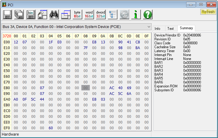
All put together, the pxpcap register bytes should read 0x10, 0x00, 0x91, 0x00. Looking at the IMC device on bus 0x3A, I was able to see that this was the case:

I repeated the same check for device 12 (0x0C) and found that it showed the same data at that address. The device/vendor ID was also consistent – 0x8086 / 0x2040. Knowing this makes it easier to find the IMC devices in future.
The next thing I wanted to check was whether there was any chance that TSOD or CLTT were enabled. The first register to look at was smbcntl_[0:1], which contains a field called SMB_DTI:
SMB_DTI(smb_dti):
Device Type Identifier: This field specifies the device type identifier. Only devices with this device-type will respond to commands.
‘0011’ specifies TSOD.
‘1010’ specifies EEPROMs.
‘0110’ specifies a write-protect operation for an EEPROM.
Other identifiers can be specified to target non-EEPROM devices on the SMBus.
Note: IMC based hardware TSOD polling uses hardcoded DTI. Changing this field has no effect on the hardware based TSOD polling.–
smbcntl_[0:1]/ SMB_DTI register field documentation, page 26 of the Intel Xeon Scalable 2nd Generation Datasheet (Vol. 2)
I say “the” register, but there are actually two – one at offset 0xE88 and one at 0xE98, matching each triplet of memory channels.
The note explains why the folks at PassMark considered it problematic. If TSOD polling is enabled, the IMC may take over the SMBus whenever the polling interval elapses, causing SPD EEPROM reads to fail.
If the data in the high nibble of the last byte of the register is 0b1010 (0xA), then the bus is used for SPD EEPROM devices. If it’s 0b0011 (0x03) then the bus is used for TSOD sensors.
The high nibble is 0xA, so it’s being used for SPD EEPROMs, not TSOD.
The low 8 bits of the same register contain a field called TSOD_PRESENT. Since both 0xE88 and 0xE98 are zero bytes, this indicates that there are no TSOD devices present. I verified this for both IMCs on both CPUs.
Reading a little further into the details, Closed Loop Thermal Throttle (CLTT) may also be an issue since it can perform SMBus reads at any time during temperature polling. The configuration of CLTT vs. OLTT (closed vs. open) can be checked via the chn_tmp_cfg registers, which are at offset 0x108 of bus B(2), devices 10, 11, and 12, functions 2 and 6. This means that, in total, on my system, there are actually 12 of these registers: two functions in each of three devices on two CPUs.
In each case the byte at offset 0x108 turned out to be 0xF4. This indicates that OLTT is enabled, not CLTT, so we should be ok.
Interesting side-note here: DIMMs still appear to report high-resolution cumulative energy consumption at offset 0x7C of bus B(1), device 0x1E, function 0x02, as part of RAPL power reporting services, despite the equivalent MSR being patched to reduce its access rate when SGX is enabled, in order to mitigate PLATYPUS. This is possibly a bug – I’ll email Intel about this.
Looking a little further back in the spec, I also noticed that SMB_SBE (SMBus Error flag) at bit 29 of offset 0xE80 in the above screenshot is not set. This is good news – the bus is not in an error state.
All of this comes together to show that DIMM SPDs can indeed be accessed through the IMC interface, and the only thing stopping us is that none of the existing tools have explicit support for it. Luckily, however, there’s a BSD library called imcsmb that does have support.
The transfer process is roughly as follows:
- Save the value of
smb_cntlfor later restoration. - In a local copy of
smb_cntl, clear thesmb_dtifield and set it to the top 4 bits of the SPD EEPROM address. This will almost always be 0b1010 for us since we’re addressing EEPROMs, but there is an exception I’ll mention later. - Set the
smb_ckovrd, to enable normal SMB operation. - Clear the
smb_dis_wrtbit. I’m not sure if this is strictly necessary, since this should not be writable outside of SMM, but the imcsmb implementation claims that the real behaviour is counter to the datasheet’s documentation. - Clear the
smb_tsod_poll_enbit, to disable TSOD polling (if enabled) and enable access tosmbcmd. - Build an
smbcmdcommand value:- Set the
smb_cmd_triggerbit. - Set the
smb_word_accessbit set if we’re reading 2-byte words instead of bytes. - Clear the
smb_wrt_cmdfield cleared (this is a read) - Set
smb_sato bits [3:1] of the SPD EEPROM address. The top four bits of the address are the DTI, as in step 2, and the bottom bit of the address is the read/write bit. This leaves [3:1] as the select address. - Set
smb_bato the 8-bit address offset to be read from the SPD EEPROM.
- Set the
- Write the
smb_cntlregister to PCI. - Poll until the
smb_busybit of thesmb_statregister is cleared. If this is not cleared within 35ms, there was a timeout – restore the originalsmb_cntlvalue and return. - Write the
smbcmdregister to PCI. - Poll until the
smb_rdo(read data valid) bit in thesmb_statregister is set to 1. If this is not set within 35ms, there was a timeout – restore the originalsmb_cntlvalue and return. - Check that the
smb_sbe(SMBus Error) bit is not set. If it is, there was an SMBus error – restore the originalsmb_cntlvalue and return. One thing of note is that the error bit is always set for EEPROM page-change operations. - Read the
smb_rdatafield out ofsmb_stat. For single byte reads the data is returned in [7:0]. For 2-byte word reads the data takes up the full [15:0] space, but the byte order must be swapped.
One thing that’s important to point out is that only a single 256-byte page of SPD EEPROM data can be accessed at one time, but there are actually 512 bytes of flash on the chip. If you think back to earlier, where I quoted the Device Type Identifier (DTI) field definition that decided whether an EEPROM or TSOD device was being accessed (0b1010 or 0b0011), you may also remember that there were other possible values for the DTI. One of those is 0b0110, which is specified as a “write-protect operation”. This isn’t a very helpful description, since the 0b0110 prefix is actually more of a generic command interface specifier; write-protect is just one of the things it can do. We can take a look at the SPD command set for the details:

The important commands here are “Set SPD Page Address to 0 (Select Lower Bank)” and “Set SPD Page Address to 1 (Select Upper Bank)”. For both commands we set the DTI (preamble) to 0b0110. To switch to the lower bank (i.e. the first 256 bytes) we set the address in smb_sa to 0b110, and to switch to the upper bank we set the address to 0b111. The transfer process is executed as normal, but no data is returned and the smb_sbe error flag might be set even if there was no actual error. The reason for the error flag behaviour appears to be due to some errata in certain SPD flash chips where some of them do specify an ACK bit at the end of the SMBus transaction, but others do not.
I wrote an RW Everything script to go through the process, but I haven’t managed to get it working. Everything seems to work as expected, but neither the smb_rdo or smb_sbe bits get set after the command is written.
LocalF0 is the select address of the DIMM (0 to 7)
LocalF1 is the offset in the SPD memory to read (0x00 to 0xFF)
LocalF2 is the device to read from (0x0A for IMC0, 0x0C for IMC1)
LocalF3 is the smbcntl register offset to use (0xE88 or 0xE98)
LocalF4 is the smbcmd register offset to use (0xE84 or 0xE94)
LocalF5 is the smb_stat register offset to use (0xE80 or 0xE90)
> LocalF0=2;
> LocalF1=0x00;
> LocalF2=0x0A;
> LocalF3=0xE88;
> LocalF4=0xE84;
> LocalF5=0xE80;
> cout Check if Ubox is present...;
> Local0=Rpci32(0,0x08,2,0);
> bkif1(Sub(Local0,0x20168086));
> cout Read CPUBUSNO2...;
> Local0=Rpci32(0,0x08,2,0xCC);
> Local0=Shr(Local0,16);
> Local0=And(Local0,0xFF);
> cout CPUBUSNO2 is 0x%L0h;
> cmds { bkif1(Local0); cout Invalid CPUBUSNO2 value.; exit; }
> cout Read IMC VID/DID...;
> Local1=Rpci32(Local0,LocalF2,0,0);
> cout Check IMC VID/DID...;
> cmds { bkif0(Sub(Local1,0x20408086)); cout IMC VID/DID does not match expected.; exit; }
> cout IMC found.
> Local90=Rpcie32(Local0,LocalF2,0,LocalF3)
> cout Original smbcntl_0 register value is 0x%L90h;
Mask DTI bits
> Local4=Shl(0b1111,28)
> Local4=Not(Local4)
> Local3=And(Local90,Local4)
Set DTI bits
> Local4=Shl(0b1010,28)
> Local3=Or(Local3,Local4)
Set override bit
> Local4=Shl(1,27)
> Local3=Or(Local3,Local4)
Clear write disable bit
> Local4=Shl(1,26)
> Local4=Not(Local4)
> Local3=And(Local3,Local4)
Clear TSOD polling bit
> Local4=Shl(1,8)
> Local4=Not(Local4)
> Local3=And(Local3,Local4)
> cout New smbcntl_0 register value is 0x%L3h;
> cout Building smbcmd_0 register...
> Local5=0
Set trigger bit
> Local4=Shl(1,31)
> Local5=Or(Local5,Local4)
Set SA bits
> Local4=Shl(LocalF0,24)
> Local5=Or(Local5,Local4)
Set BA bits
> Local4=Shl(LocalF1,16)
> Local5=Or(Local5,Local4)
> cout New smbcmd_0 register value is 0x%L5h;
> cout Writing smbcntl_0...
> wpcie32(Local0,LocalF2,0,LocalF3,Local3);
> wait { 0, 35, LocalF=rpcie32(Local0,LocalF2,0,LocalF5); Local21=Shl(1,28); And(LocalF,Local21); }
> cout Writing smbcmd_0...
> wpcie32(Local0,LocalF2,0,LocalF4,Local5);
> wait { 1, 35, LocalF=rpcie32(Local0,LocalF2,0,LocalF5); Local21=Shl(1,31); Local22=Shl(1,29); Local23=And(LocalF,Local21); Local24=And(LocalF,Local22); Or(Local23,Local24); }
> cout SMB status is %L20h
> cout RDO = %L23h, SBE = %L24h
> Local22=And(LocalF,0xFF)
> cout Data byte is %L22h
> cout Restoring original smbcntl_0 value...
> wpcie32(Local0,LocalF2,0,LocalF3,Local90);
> cout Done.
The output is as follows:
> LocalF0=2;
LocalF0 = 0x0000000000000002 (2)
> LocalF1=0x00;
LocalF1 = 0x0000000000000000 (0)
> LocalF2=0x0A;
LocalF2 = 0x000000000000000A (10)
> LocalF3=0xE88;
LocalF3 = 0x0000000000000E88 (3720)
> LocalF4=0xE84;
LocalF4 = 0x0000000000000E84 (3716)
> LocalF5=0xE80;
LocalF5 = 0x0000000000000E80 (3712)
> cout Check if Ubox is present...;
Check if Ubox is present...
> Local0=Rpci32(0,0x08,2,0);
Read PCI Bus/Dev/Fun/Offset 0x00/0x08/0x02/0x000 = 0x20168086
> bkif1(Sub(Local0,0x20168086));
Sub (0x20168086, 0x20168086) = 0x0000000000000000
> cout Read CPUBUSNO2...;
Read CPUBUSNO2...
> Local0=Rpci32(0,0x08,2,0xCC);
Read PCI Bus/Dev/Fun/Offset 0x00/0x08/0x02/0x0CC = 0x5D3A1700
> Local0=Shr(Local0,16);
Shr (0x000000005D3A1700, 0x0000000000000010) = 0x0000000000005D3A
> Local0=And(Local0,0xFF);
And (0x5D3A, 0xFF) = 0x000000000000003A
> cout CPUBUSNO2 is 0x%L0h;
CPUBUSNO2 is 0x3A
> cmds { bkif1(Local0); cout Invalid CPUBUSNO2 value.; exit; }
Local0 = 0x000000000000003A (58)
Command break
> cout Read IMC VID/DID...;
Read IMC VID/DID...
> Local1=Rpci32(Local0,LocalF2,0,0);
Read PCI Bus/Dev/Fun/Offset 0x3A/0x0A/0x00/0x000 = 0x20408086
> cout Check IMC VID/DID...;
Check IMC VID/DID...
> cmds { bkif0(Sub(Local1,0x20408086)); cout IMC VID/DID does not match expected.; exit; }
Sub (0x20408086, 0x20408086) = 0x0000000000000000
Command break
> cout IMC found.
IMC found.
> Local90=Rpcie32(Local0,LocalF2,0,LocalF3)
Read PCIE Bus/Dev/Fun/Offset 0x3A/0x0A/0x00/0xE88 = 0xAC000000
> cout Original smbcntl_0 register value is 0x%L90h;
Original smbcntl_0 register value is 0xAC000000
> Local4=Shl(0b1111,28)
Shl (0x000000000000000F, 0x000000000000001C) = 0x00000000F0000000
> Local4=Not(Local4)
Not (0x00000000F0000000) = 0xFFFFFFFF0FFFFFFF
> Local3=And(Local90,Local4)
And (0xAC000000, 0xFFFFFFFF0FFFFFFF) = 0x000000000C000000
> Local4=Shl(0b1010,28)
Shl (0x000000000000000A, 0x000000000000001C) = 0x00000000A0000000
> Local3=Or(Local3,Local4)
Or (0x000000000C000000, 0x00000000A0000000) = 0x00000000AC000000
> Local4=Shl(1,27)
Shl (0x0000000000000001, 0x000000000000001B) = 0x0000000008000000
> Local3=Or(Local3,Local4)
Or (0x00000000AC000000, 0x0000000008000000) = 0x00000000AC000000
> Local4=Shl(1,26)
Shl (0x0000000000000001, 0x000000000000001A) = 0x0000000004000000
> Local4=Not(Local4)
Not (0x0000000004000000) = 0xFFFFFFFFFBFFFFFF
> Local3=And(Local3,Local4)
And (0xAC000000, 0xFFFFFFFFFBFFFFFF) = 0x00000000A8000000
> Local4=Shl(1,8)
Shl (0x0000000000000001, 0x0000000000000008) = 0x0000000000000100
> Local4=Not(Local4)
Not (0x0000000000000100) = 0xFFFFFFFFFFFFFEFF
> Local3=And(Local3,Local4)
And (0xA8000000, 0xFFFFFFFFFFFFFEFF) = 0x00000000A8000000
> cout New smbcntl_0 register value is 0x%L3h;
New smbcntl_0 register value is 0xA8000000
> cout Building smbcmd_0 register...
Building smbcmd_0 register...
> Local5=0
Local5 = 0x0000000000000000 (0)
> Local4=Shl(1,31)
Shl (0x0000000000000001, 0x000000000000001F) = 0x0000000080000000
> Local5=Or(Local5,Local4)
Or (0x0000000000000000, 0x0000000080000000) = 0x0000000080000000
> Local4=Shl(LocalF0,24)
Shl (0x0000000000000002, 0x0000000000000018) = 0x0000000002000000
> Local5=Or(Local5,Local4)
Or (0x0000000080000000, 0x0000000002000000) = 0x0000000082000000
> Local4=Shl(LocalF1,16)
Shl (0x0000000000000000, 0x0000000000000010) = 0x0000000000000000
> Local5=Or(Local5,Local4)
Or (0x0000000082000000, 0x0000000000000000) = 0x0000000082000000
> cout New smbcmd_0 register value is 0x%L5h;
New smbcmd_0 register value is 0x82000000
> cout Writing smbcntl_0...
Writing smbcntl_0...
> wpcie32(Local0,LocalF2,0,LocalF3,Local3);
Write PCIE Bus/Dev/Fun/Offset 0x3A/0x0A/0x00/0xE88 = 0xA8000000
> wait { 0, 35, LocalF=rpcie32(Local0,LocalF2,0,LocalF5); Local21=Shl(1,28); And(LocalF,Local21); }
Read PCIE Bus/Dev/Fun/Offset 0x3A/0x0A/0x00/0xE80 = 0x07000000
Shl (0x0000000000000001, 0x000000000000001C) = 0x0000000010000000
And (0x7000000, 0x10000000) = 0x0000000000000000
> cout Writing smbcmd_0...
Writing smbcmd_0...
> wpcie32(Local0,LocalF2,0,LocalF4,Local5);
Write PCIE Bus/Dev/Fun/Offset 0x3A/0x0A/0x00/0xE84 = 0x82000000
> wait { 1, 35, LocalF=rpcie32(Local0,LocalF2,0,LocalF5); Local21=Shl(1,31); Local22=Shl(1,29); Local23=And(LocalF,Local21); Local24=And(LocalF,Local22); Or(Local23,Local24); }
Read PCIE Bus/Dev/Fun/Offset 0x3A/0x0A/0x00/0xE80 = 0x07000000
Shl (0x0000000000000001, 0x000000000000001F) = 0x0000000080000000
Shl (0x0000000000000001, 0x000000000000001D) = 0x0000000020000000
And (0x7000000, 0x80000000) = 0x0000000000000000
And (0x7000000, 0x20000000) = 0x0000000000000000
Or (0x0000000000000000, 0x0000000000000000) = 0x0000000000000000

... snip lots of repeats ...

Read PCIE Bus/Dev/Fun/Offset 0x3A/0x0A/0x00/0xE80 = 0x07000000
Shl (0x0000000000000001, 0x000000000000001F) = 0x0000000080000000
Shl (0x0000000000000001, 0x000000000000001D) = 0x0000000020000000
And (0x7000000, 0x80000000) = 0x0000000000000000
And (0x7000000, 0x20000000) = 0x0000000000000000
Or (0x0000000000000000, 0x0000000000000000) = 0x0000000000000000
> cout SMB status is %L20h
SMB status is 0
> cout RDO = %L23h, SBE = %L24h
RDO = 0 SBE = 0
> Local22=And(LocalF,0xFF)
And (0x7000000, 0xFF) = 0x0000000000000000
> cout Data byte is %L22h
Data byte is 0
> cout Restoring original smbcntl_0 value...
Restoring original smbcntl_0 value...
> wpcie32(Local0,LocalF2,0,LocalF3,Local90);
Write PCIE Bus/Dev/Fun/Offset 0x3A/0x0A/0x00/0xE88 = 0xAC000000
> cout Done.
Done.
Perhaps someone will spot my mistake. For now I don’t really have any more time to work on it. At least I figured out this much, though.
I’m in touch with the folks at PassMark, so hopefully we can get the Skylake Xeon IMC working in RAMMon at least. If anyone knows any of the devs at CPUID, I’d be happy to talk to them too.
Recommend
-
38
README.md Twitter Network Layer (a.k.a TNL) The Twitter Network Layer (TNL) is a framework for interfacing with the
-
7
Menu Linear scalable read-write lock Lu Pan | 01 Jul 2020 | 5 min read
-
8
Hacked On SO-DIMM Slot Was Worth A Shot Finding unpopulated pads on a circuit board is often a sign that the device in question has some untapped potential. These blank spots on...
-
12
3rd gen Intel Xeon Scalable processors available at...
-
5
Intel Discloses Multi-Generation Xeon Scalable Roadmap It’s no secret that Intel’s enterprise processor platform has been stretched in recent generations. Compared to the competition, Intel is chasing its multi-die strategy while rely...
-
4
Raspberry Pi CM3E joins CM4S in the old SO-DIMM form factor June 14, 2022...
-
1
Intel plots a path to ‘universal AI’ with 4th Gen Xeon Scalable CPU
-
11
Azure Confidential Computing on 4th Gen Intel Xeon Scalable Processors with Intel TDX Posted on January 10, 2023
-
8
Dell announces new PowerEdge servers based on Intel's 4th Gen Xeon Scalable processors
-
4
iAPX432 : Gordon Moore, Risk and Intel’s Super-CISC failureThe legacy of Intel's over-ambitious 32-bit 'micromainframe' failure.
About Joyk
Aggregate valuable and interesting links.
Joyk means Joy of geeK