

AMD's next compute GPU could have two dies and 128 GB of memory | TechSpot
source link: https://www.techspot.com/news/90293-amd-next-compute-gpu-could-have-two-dies.html
Go to the source link to view the article. You can view the picture content, updated content and better typesetting reading experience. If the link is broken, please click the button below to view the snapshot at that time.
AMD's next compute GPU could have two dies and 128 GB of memory
And it's coming soon
By Isaiah Mayersen July 3, 2021, 11:24 AMFun fact: Aldebaran is the brightest star in the Taurus constellation. It’s 44 times the size of the sun and 400 times as luminous. It’s also the namesake of AMD’s next Instinct Accelerator.
Aldebaran, the computer part, has appeared a few times in Linux patch notes. Its two-die design was half-implied in February and confirmed last month: "on Aldebaran, only primary die fetches valid power data. Show power/energy values as 0 on secondary die," one note reads.
It’s the first AMD Accelerator/GPU to leverage an MCM (multi-chip module) design, a technique that’s been plastered on patents for years but has only just begun to materialize. Using multiple chips/dies connected closely allows for more scalability than traditional monolithic designs, but also reduces the per-compute unit performance of a card, particularly in poorly parallelized workloads.
Nvidia is expected to challenge Aldebaran with their own MCM designs based on the Hopper architecture next year. Intel, meanwhile, is on the verge of releasing the Ponte Vecchio accelerator based on the Xe HPC architecture and an early MCM implementation.
Like Ponte Vecchio, Aldebaran leverages MCM to expand memory capacity, patch notes imply. A note from last week describes Aldebaran as having two dies, four UMCs per die, and eight channels connected to 2 GB of HBM per UMC. Or 128 GB, in total.
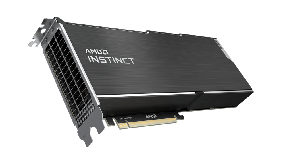
AMD's surprisingly edgy MI100.
The patch notes also mention support for a "new HBM2 memory type," presumably HBM2e. If AMD is using SK Hynix’s new HBM2e memory modules with 3.6 Gbps of bandwidth and a 4096-bit bus on each die, then Aldebaran could have 3.6 TB/s of memory bandwidth.
For comparison, Aldebaran’s predecessor, the Instinct MI100 (formerly codenamed Arcturus, another star) has 32 GB of HBM2 and 1.2 TB/s of memory bandwidth. Nvidia’s A100 accelerator can be configured with up to 80 GB of 3.2 Gbps HBM2e memory for 2 TB/s of bandwidth.
AMD CEO Dr Lisa Su has already said that the CDNA2 architecture, meaning Aldebaran, is slated for release later this year. Presumably, it will release as the MI200 Accelerator.
"This year, as I said, we’re putting together our next generation CDNA architecture. This is actually a key component that enabled us to win the largest supercomputer bids in the US," Su said at a conference in May. "… And we will be launching the next generation of that architecture, actually, later this year. We’re very excited about it. I think it’s progressed extremely well."
Masthead by Timothy Dykes
Recommend
About Joyk
Aggregate valuable and interesting links.
Joyk means Joy of geeK