

Modern CPUs have a backstage cast
source link: https://www.devever.net/~hl/backstage-cast
Go to the source link to view the article. You can view the picture content, updated content and better typesetting reading experience. If the link is broken, please click the button below to view the snapshot at that time.
Modern CPUs have a backstage cast
If you take someone with intermediate knowledge of computing in the right areas, and ask them how an x86 machine boots, they'll probably start telling you about how the CPU first comes up in real mode and starts executing code from the 8086 reset vector of FFFF:FFF0. This understanding of how an x86 machine boots has remained remarkably persistent, as far as I can tell because this basic narrative about the boot process has been handed down from website to website, generation to generation, largely unchanged.
It's also a pack of lies and hasn't reflected the true nature of the boot process for some time. It's true the 8086 reset vector is still used, but only because it's a standard “ABI” for the CPU to transfer control to the BIOS (whether legacy PC BIOS or UEFI BIOS). In reality an awful lot happens before this reset vector starts executing.1 Aside from people having vaguely heard about the Intel Management Engine, this modern reality of the boot process remains largely unknown. It doesn't help that neither Intel nor AMD have really gone out of their way to actually document what the modern boot process looks like, and large parts of this process are handled by vendor-supplied mystery firmware blobs, which may as well be boxes with “???” written in them. Mainly we have the substantial assistance of assorted reverse engineers and security researchers to thank for the fact that we even have a decent picture of what the modoern x86 boot process actually looks like for both Intel and AMD. I could write a whole article about that process — but instead, I'd like to focus on something else.
Basically any multiprocessor CPU chip of reasonable sophistication produced today — i.e., desktop and server CPUs, and probably smartphone SoCs for that matter, also has an entire “backstage cast” of ancillary support cores keeping things running correctly. Some of these mainly handle the boot process, and we're more likely to know about these (e.g. Intel ME/AMD PSP), but even less known are “backstage” cores which don't participate in the boot process but which are instead involved in things like power and thermal regulation.
Intel and AMD x86 platforms confer a distinct sense of “pay no attention to the man behind the curtain” in their design, essentially trying to conceal the existence of these ancillary cores. AMD CPUs, for example, not only have the PSP, but also have an ancillary core known as the System Management Unit (SMU). Before Zen it used the LM32 ISA, now it uses the Xtensa ISA. Some references seem to suggest that modern AMD CPUs actually have multiple SMUs, with different responsibilities, but it's hard to confirm this. The conclusion here is that I don't even actually know how many of these SMUs a modern AMD CPU has. Moreover, we just happen to have managed to find out about AMD's SMU; does Intel have an equivalent, more effectively hidden? Probably, though I don't know.
Intel CPUs have something called the CRBus, which is an internal memory bus for access to control registers with its own address space. You can't access this address space directly; your access to it is locked down. The CRBus is used by the Intel ME to control CPU settings Intel doesn't want you to be able to twiddle directly; I believe CPU microcode is also able to access this bus, so that MSR reads and writes (for example) can essentially be implemented as proxied, and highly restricted, access to particular registers mapped on the CRBus. Intel doesn't document the existence of the CRBus anywhere, and ordinarily you would never know of its existence; we only know of its existence due to the work of some extraordinary hackers. This is another example of “pay no attention to the man behind the curtain”. It's quite fascinating how on modern CPUs is how there is almost always a deeper level of system innards, but which is invariably hidden behind the simulacrum of pretending that the hardware is no different than a Pentium III. In the x86 case, the “curtain” has been quite strongly reinforced by vendors — and had the letters “‘hardware’ (honest)” painted on it.
One of the most interesting things ever to happen in the open source firmware space, the release of Raptor's Talos II/Blackbird POWER9 systems, created an interesting opportunity here. For the first time, we got to see what a modern server CPU really looks like behind the scenes. What makes the POWER9 CPUs really interesting is that there is no “curtain” in the design of POWER9. The POWER9's equivalent to Intel's CRBus, which is known as SCOM, rather than being a secret the very existence of which is omitted from mention, is instead openly accessible.2
Even more interestingly, however, we have an exhaustive picture of the entire “backstage cast” of the POWER9 CPU. These are all the ancillary support cores responsible for system boot, power and thermal regulation and other functions that need to go on in the background while the system is running:
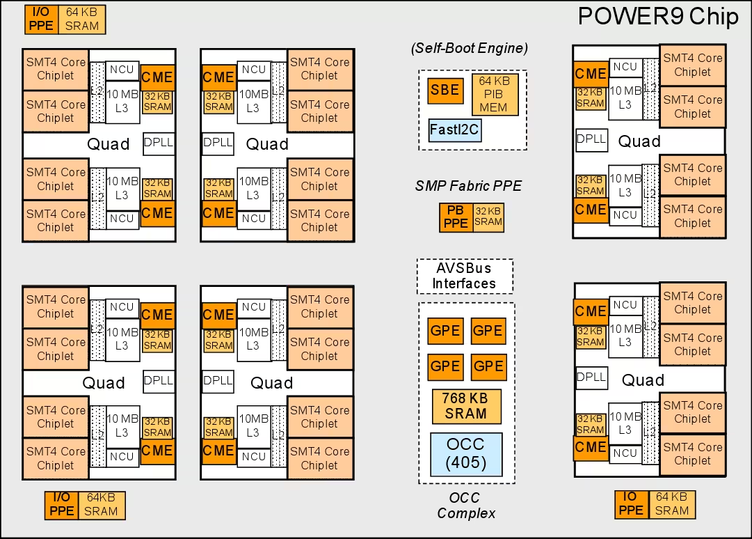
POWER9 PPE Instances
Let me break this down:
Each “SMT4 Core Chiplet” (quantity: 24) is a single core of the 24-core chip, with 4-way multithreading. These are, of course, the stars of the show.
The Self-Boot Engine (SBE) (quantity: 1) is a core which is responsible for booting the entire system. It's responsible for initialising the chip and getting it out of bed enough to the point where at least one of the main cores can run using cache-as-RAM mode; it does little after that point. It has some SRAM to do its work in and uses a slightly custom variant of the 32-bit Power ISA, extended to support 64-bit loads and stores using adjacent GPR pairs. This core design is known as a PPE. It's the first thing that runs on the CPU die.
In this regard its function is basically identical to that of the Intel ME or AMD PSP, except that its firmware is open source and owner-controllable rather than being a vendor-signed binary blob (plus it doesn't have DRM functionality).
The On-Chip-Controller (OCC) (quantity: 1) is a PPC 405 core which is responsible for power and thermal monitoring. It communicates with a BMC to give it temperature readings and therefore allow the BMC to determine how fast to run the fans. The OCC can also choose a power envelope limit — e.g. you could tell it to limit power consumption to 65 W, or similar. It's basically an endless control loop.
The General Purpose Engines (GPE) (quantity: 4) exist to support the OCC, and are controlled by it. These are split into pstate GPEs (PGPEs) and STOP GPEs (SGPEs). As the names imply, pstate GPEs relate to power state management, and STOP GPEs relate to CPU sleep management.
The Core Management Engine (CME) (quantity: 12) uses the same stripped-down Power ISA variant as the SBE. Each CME is responsible for a pair of cores. Its responsibilities are related to power management of the core, core sleep states, etc.
I/O PPEs (quantity: 3), which manage CAPI-related functions and therefore aren't used on most systems. (CAPI is a cache coherent interconnect protocol created by IBM which can run over PCIe or NVLink; in this regard it's essentially a predecessor to the current CXL initiative.)
The Pervasive Bus PPE (PB PPE) (quantity: 1), which to my knowledge is unused, at least on the Talos/Blackbird systems.
This means that the total number of cores on an IBM POWER9 chip is:
- 1x SBE (PPE Power ISA variant);
- 12x CME (PPE Power ISA variant);
- 4x GPE (PPE Power ISA variant);
- 3x IOPPE (PPE Power ISA variant);
- 1x PBPPE (PPE Power ISA variant);
- 1x OCC (PPC405);
- 24x POWER9 Cores
summing to 22 ancillary backstage cores, or 46 cores in total. Thus, almost half of the cores on the CPU module are actually part of the backstage cast! The “main” cores of a POWER9 CPU are just the tip of the iceberg.
The reason this is interesting is because POWER9 is basically the first time the public got a real view of how sophisticated the backstage cast actually is of a modern server CPU. It's quite likely that Intel and AMD x86 CPUs look very similar nowadays, and we just don't know about the sheer extent of the “backstage cast” because it's all kept behind the curtain. In other words, POWER9 is not an oddity but a revelation as to what modern CPUs look like.3
See also: An interesting article about Bunnie on economic forces that encourage closed hardware.
1. It's actually even more comical. On modern Intel platforms with Boot Guard enabled, after the Intel ME stage, one of the main cores then starts executing the Intel “Authenticated Code Module” (ACM), another Intel-signed proprietary binary blob, which is responsible for implementing secure boot. Since this blob is presumably not real-mode code, it inevitably switches the CPU into protected mode to execute... then switches it back into real mode when it's time to execute the motherboard vendor's BIOS by jumping to the traditional reset vector — which will of course switch the CPU back into protected mode just a few instructions later. ⏎
2. There's probably a reason POWER9 is so “unlocked” relative to your average x86 CPU, and I think I know what it is: For Intel and AMD, the demarcation point between them and their customer is the CPU, so if they want to keep secrets and maintain a stable interface between them and their customers, they're effectively pushed to do it at the CPU boundary. With IBM, this historically hasn't been the case; traditionally, IBM has only sold servers containing their own CPUs, not the CPUs alone. This means that traditionally, the only customer for IBM CPUs has been IBM — which means there's far less motivation for IBM to lock things down. Moreover, IBM Power servers have traditionally shipped with a proprietary hypervisor (known as PowerVM) built into the firmware. On these servers, all OSes run under this hypervisor, and you can't run an OS directly on the bare metal. This means that the natural interface between IBM and its customers has naturally fallen at the hypervisor—OS interface, not at the CPU. In fact, traditionally even the initialisation of the PCIe I/O subsystem was part of the PowerVM hypervisor — when IBM created the OpenPOWER platform (which doesn't have this hypervisor and actually does boot to bare metal), they had to extract this PCIe initialisation code into a new open source firmware component that runs before bare-metal Linux. Thus, the natural “pay no attention to the man behind the curtain” demarcation of IBM Power systems has always been at the hypervisor—OS line, not the CPU—hypervisor line. Indeed, many of the enterprisey DRM features IBM implements in their own Power servers (“capacity on demand” and so on) are found in their PowerVM hypervisor. When IBM suddenly decided to open up their POWER CPUs for use by third parties, they made available a platform which for its entire lifespan up until that point, hadn't evolved under the same pressures as the existing x86 CPU market, but instead in an environment in which there was really no natural motive for them to lock things down at the CPU level. Which is almost certainly why IBM POWER CPUs seem to so greatly lack any “curtains” — the curtain had always been shipped with the hypervisor, not the CPU. ⏎
3. There are of course other cores on the Talos II/Blackbird POWER9 systems. These include:
- the AST2500 bog-standard BMC SoC, which has an ancient ARM1176JZS main core but also a supporting Coldfire microcontroller core, which uses a variant of the Motorola 68000 ISA;
- the BCM5719 NIC, which I know way too much about, which has four ancient MIPS (roughly MIPS II) cores and one ARM Cortex-M3 core.
If you include these, there are 29 supporting cores or 53 total cores in a single-socket system. There's also a small iCE40 FPGA for power sequencing (and no, there aren't any softcores hosted on it).
On Blackbird systems I believe there may be an ARM core on the SATA controller chip which is unused (probably intended for hardware RAID applications). On the Talos II there is an external fan control chip; the vendor's datasheet describes this as using a RISC CPU internally, which runs only from a completely hardcoded mask ROM. Thus this is essentially just an implementation detail, but you can count it if you like. The Talos II can be ordered with an optional onboard Microsemi PM8068 SAS chip (not recommended), in which case there is proprietary firmware running on at least one MIPS core, and possibly more. ⏎
Recommend
-
76
README.md
-
26
README.md D2Admin 是一个开源的管理系统前端集成方案,为了方便开发者快速进行管理系统开发而设计 仓库和文档 本项目仓库在 Github 和 Gitee 同步发布
-
61
README.md D2Admin 是一个开源的管理系统前端集成方案,为了方便开发者快速进行管理系统开发而设计 仓库和文档 本项目仓库在 Github 和 Gitee 同步发布
-
24
Android Developers Backstage
-
17
Backstage What is Backstage? Backstage is an open platform for building developer portals. The philosophy behind Backstage is simple: Don't expose you...
-
8
How AvionDB P2P Data Syncing Works Backstage?Responses
-
5
CoinGeek Backstage: Steven Zeiler and Derrick Horton Interviews 22 December 2020...
-
9
Announcing the Backstage Stability Index · Backstage Service Catalog and Developer PlatformTL;DR Backstage is heading out of alpha and moving onto the path to stable releases and an eventual version 1.0. As the community and...
-
8
CoinGeek Backstage: Zach Resnick and Jackson Laskey Interviews 29 December 2020...
-
6
Beware: Intel 10th, 11th, 12th Gen CPUs have ÆPIC flaw that does not need side channels...
About Joyk
Aggregate valuable and interesting links.
Joyk means Joy of geeK