

LaCie 1big Dock Teardown and Review – U.2 for all?
source link: https://dancharblog.wordpress.com/2023/05/15/lacie-1big-dock-teardown-and-review-u-2-for-everyone/
Go to the source link to view the article. You can view the picture content, updated content and better typesetting reading experience. If the link is broken, please click the button below to view the snapshot at that time.
This article, by Leaves, has been adapted for English-language audiences and re-posted with permission.
Introduction
Although the LaCie Lacie 1Big Dock is quite interesting, I didn’t have the idea of buying one to disassemble at first… that is until I found out that there are quite a few folks purchasing expensive U.2 storage docks like the WERO U.2 Dock.

So we’ll look at LaCie’s competing products
Brief introduction about LaCie:
This brand has been acquired by Seagate, so products are equipped with Seagate HDD. Most of LaCie’s products are mobile hard drives and tiny storage docks. The products are high priced using premium materials and are usually purchased by studios or used by affluent folks at home or in the office.
At present, it seems that some studios have closed down or retired certain Lacie products as there are sources for used specimens at low prices.
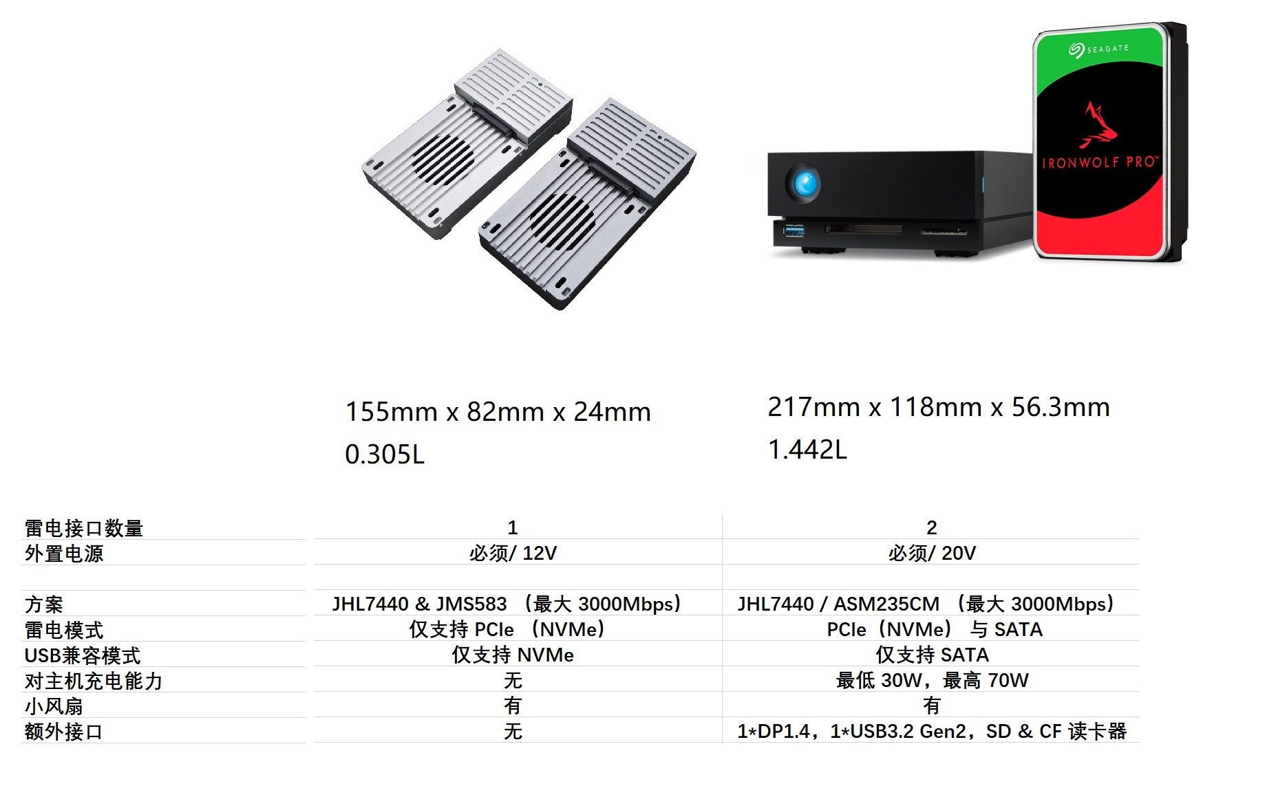
A brief comparison of the two docks is below.
Going through LaCie’s own manual:

It can be seen from glancing inside that this 1big Dock is quipped with a SFF8639 U.2 port and 7 high-speed differential pairs can be clearly seen on the PCB – so it must have 4x PCIe lanes and be the full U.2 spec – not just some version of SATA.
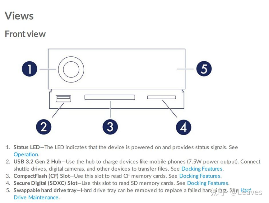
It is also equipped with DP1.4 interface, supports USB connection, and comes with a bunch of card readers in addition to the disk itself.
Well, for a veteran like me, it is a must-have to expose all available interfaces and be compatible with all listed functions. It is even better to make the most use of existing functions on a chipset (add card readers, LAN Ports etc.). But for novices, there may be different expectations. Its a storage dock which equipped with a video output port – and odd configuration.
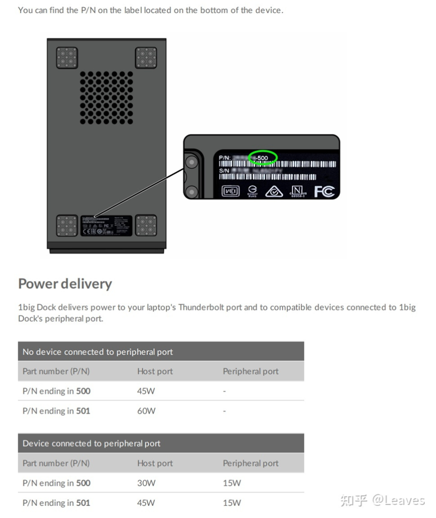
The most fancy thing is this power supply function
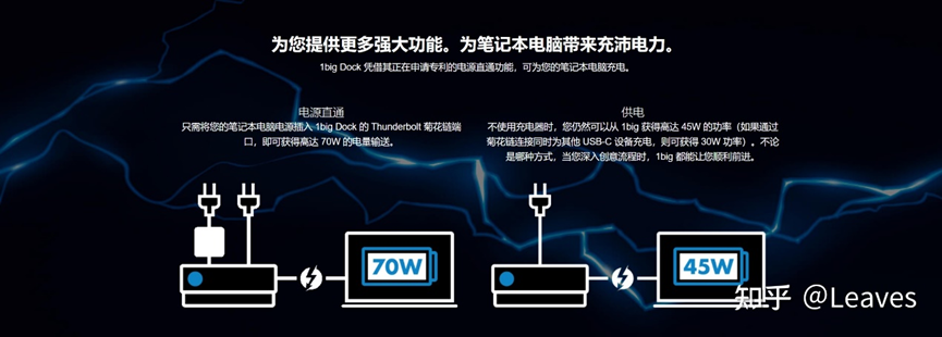
Models P/N NO. ending with 500 support combining the DC power port and the downstream Thunderbolt 3 port power to provide up to 70W to the host laptop. But 501 models do not and are limited to 45W. Of course, there is a caveat. The DC round port power supply must be plugged in to make the device run at all. So maybe the adding a bit of power with the Thunderbolt port is not so useful, so it is no wonder it was dropped for later models.
But if the LaCie is placed in a daisy chain system, it can accept power from the downstream devices and relay that back to the host PC so this is still a good power supply enhancement solution – but LaCie still hasn’t perfected the functionality.

There is a successor to the 1Big Dock, the 1Big Dock Pro. But it is the same with just different printing on the chassis indicating “SSD” and different placements for the front card readers.
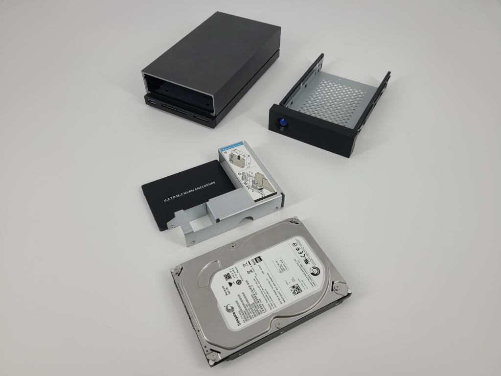
In some other evaluations, it can be seen that a 3.5-inch U.2 disk is stuffed in the disk holder – in this case it is labelled as a FireCuda.
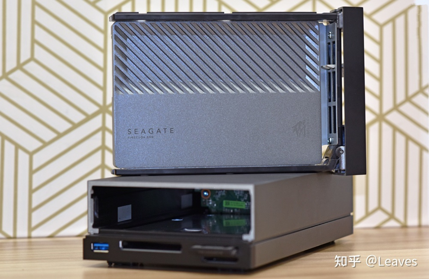
Seagate has the Nytro 5000 series disk products, but they are all 2.5″ and would not be branded as FireCuda.
After disassembling, we see an NVME M.2 SSD with a U.2->M.2 adapter.
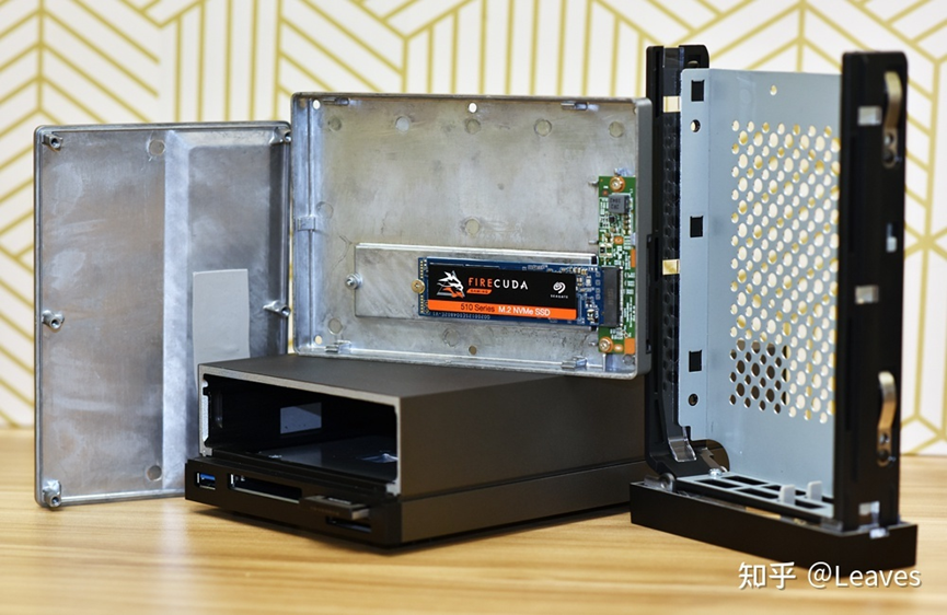
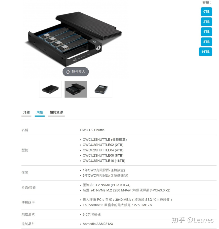
It is indeed an effective use of the old design, but not “LaCie” style, and it is too perfunctory for users who spend so much money. It is only decent if it is equipped with an OWC U2 Shuttle or similar.
Solution Prediction
Well, since a DP1.4 port is provided, and this cabinet is Thunderbolt 3 instead of Thunderbolt 4, it must be based on JHL7440. However, it is difficult to say whether the PD controller is the solution of TI or Cypress. The DP and PCIe links are directly exposed to the external interface and the built-in interface respectively, but there are many possibilities for the USB portion.
The cabinet guarantees the functions under the USB connection, and can provide a USB 3.2 Gen2 interface. It must be equipped with a USB3.2 Gen 2 Hub, but I am not sure if it is from Realtek, MicroChip or other manufacturer.
There must be a USB-to-SATA solution downstream of the Hub. According to LaCie’s habit, it should be ASMedia ASM235CM, and there is also a USB card reader solution, but I am not familiar. It is estimated more likely from Realtek. Of course, no guarantee that there is only one hub in the entire cabinet; it is also possible to connect a 5Gbps Hub downstream of the 10Gbps Hub for card readers.
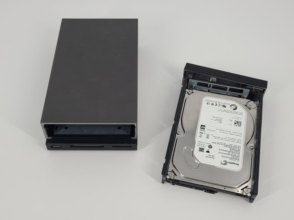
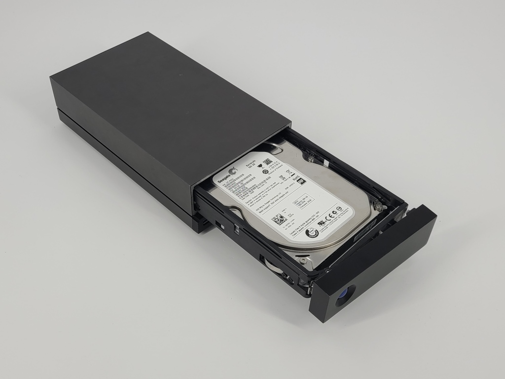
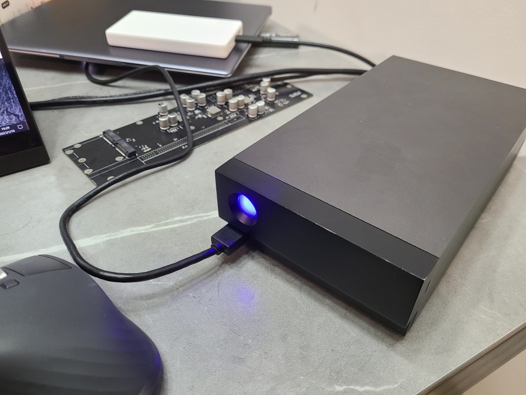
Unboxing


The label on dock says 10T and the box is marked 4T. But it’s second-hand anyway, so it doesn’t matter.


Time for LaCie’s ancestral blue eyes be replaced. It looked really cool in 2011, but now it looks a bit old-fashioned.


Teardown
Before dismantling, I thought there would be some connector at the bottom of drawer for the blue light. After closing, it connects to the LED on the drawer, and light on. But after pulling it out, it was found to be a light guide mechanism.

I have little to comment on the drawer, and I am not a NAS user, no disk cabinet used before. There are transparent light guide mechanisms on both sides of the drawer. I don’t know why they have to be placed on both sides.


Remove the rear cover and you can see there are aluminum shielding stickers around Thunderbolt port and DP.

Remove the cover from the front card reader section.

Then it can be pulled out from the rear as a whole. Note that the two wings of the black plastic part have snaps that will get stuck on the shell.

There are guide rail mechanisms on the left and right inner edges of the lower part of the shell for installing.

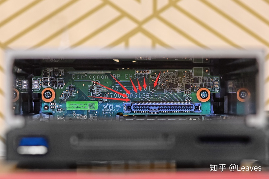
The content is easily decomposed into two parts, the upper part is the hard disk backplane fixed on the plastic part, which is only connected to the lower part through a golden finger connector. This structure is really easy to break if it is not fixed by the shell
The lower part is the PCB wrapped in a complete shielding shell. need to disassemble further.

The main body of the JHL7440 chip can be seen through the grille on the case. It seems that the small fan is not just for cooling the disk but for the JHL7440 as well through the vents.

On the back, you can see another golden finger connector similar to PCIe; it seems that the card reader part and the main body of the Thunderbolt board are designed in two sections.

Backplane Isolation and close-up. The complexity of this backplane exceeded my expectations.


This plastic part roughly acts as an outer frame, fixing the fan and the sleep button.

Now for the main course, detaching the lower shielded part. I saw the traces of aluminum foil stickers on the head and tail of the shielding shell before, and thought that the inside was directly wrapped with a layer of stickers, but in fact it only covered the IO part.
The shape of this card reader board is eye-catching The only IC on the board is specially designed with thermal pad on the shielding shell. It seems that this card reader solution is also a big heat generator.


Completely separate shielded housing. The Thunderbolt board part is completely covered by the thermal shielding sticker, but the card reader part is not. But there is only one tiny IC on the back of the card reader board.


Close-up of the Thunderbolt board after it is completely separated.


IC Tracking
Generally speaking, there are not many functional IC


PCB Analysis
4 Lane DP Main Link from JHL7440
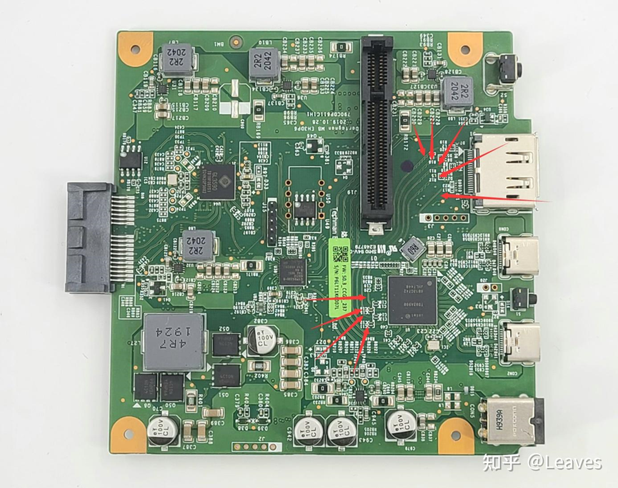
For the 4 Lane PCIe led from JHL7440, the front differential pair wiring has differential capacitors, which are TX pairs, and the reverse differential pairs are all RX, and the adjacent one with more twists should be the clock wire.


The wiring logic of GL3590 is more difficult to track.

It seems that the wiring connecting the USB Hub to the JHL7440 is on the inner layer and cannot be traced.


As for the downstream part of GL3590, it is relatively clear. It can be seen that the Hub outputs 6 differential pairs to the downstream golden finger socket, three on each side of the key; it seems to provide two complete 10Gbps USB for this socket.
On the backplane slot part, you can see two high-speed differential pair wiring, connected to an empty pad that seems to be an ESD or re-driver device, and then plugged into the socket.


For the backplane part, with the help of the SFF8639 slot pinout, you can deduce the wiring.

Wiring from U.2 socket top contacts are all PCIe.

The USB link wiring for the ASM235CM is a bit more obscure.


SATA link provided by ASM235CM to U.2 socket.

MCU communication generally uses I2C, SMB and other low-speed communication, so there will not be such conspicuous wiring as differential pairs, so I won’t track it here
A noteworthy detail is that there are actually 4 LEDs on the back panel, but only the upper left one lights up blue. The manual indicates other lighting functions, but they were not turned on in the test.


The wiring of the card reader board is basically on the inner layer, but the design logic should be very straightforward, two complete USB links, one directly plugged into the port , and the other plugged into the card reader.
It seems that LaCie’s design department was wary of the long wiring and added a re-driver chip for the USB port.

Functional Verification
Benchmarking
First come a wave of exciting benchmarks. Although I don’t have a U.2 disk, I can use the SN750 500G version to convert it into a 2.5-inch U.2, and then fix it with a 3.5-inch disk holder.

Since part of SSD has been written, the sequential writing performance has basically reached the peak. But as a JHL7440 solution, the theoretical upper limit of the write speed is also ~3000Mbps, which is still ideal in general.

Structure check
JHL7440 is typically used with CYPD5235 as the basic Thunderbolt device structure. But a CY7C series docking station controller chip is also required to ensure USB communication and Billboard functions, otherwise Thunderbolt will not work properly.
But CY7C is not in the LaCie design. Even the Thunderbolt reference designs provided by Infineon is replaced by a bunch of controllers. So Lacie’s model, perhaps the NXP LPC11U67 MCU takes over the original CY7C function? Or is it true that LaCie’s design no longer requires a Billboard controller?
After removing the back panel, we can unplug the U.2 backplane board to find out.


After removing the backplane, the mainboard can’t work normally, even can’t support PD function, so the conclusion is that NXP’s MCU replaces the CY7C controller function, it is estimated that it is for the acrobatic power supply function that NXP’s MCU was used for development. The MCU probably also controls the fan and LEDs.
At first I thought the U.2 backplane could be redesigned so that the docking station could be recessed into some more interesting build, but that seems unlikely now.
PCIe function check
The PCIe-related wiring has been determined, so let’s go directly to an external graphics card test.
U.2 to M.2 to provide M.2 port, and then supported by ADT’s M.2 -> PCIe external graphics kit.


AMD Vega FE is running fine, Catalyst is fine, bus speed is normal PCIe 3.0 x4.
Power delivery function check
When there is no external PSU, the power is reported as 30W, but according to the manual, the PD output will drop to 30W only when the downstream Thunderbolt port is connected to an device.

After the downstream Thunderbolt port is connected to the power supply, it still reports 30W charging capacity

The second thunder port report is 15W, but here there is no support for Battery Charge

Well, this is the first time I have come into contact with such a complex charging function, and it is really difficult to have any complete testing methods. After using my notebook to connect, it can probably reach the upper limit of the notebook’s power input ~40W. So it is likely that after the thunderbolt handshake is completed, the PD configuration will be changed with a second handshake.
Topology Speculation
Compared with the docking station of HP G2, G4, LaCie’s tray is relatively straightforward.
Overall, the peripherals and performance are relatively complete.

Conclusion
I’ve been very happy with the few LaCie external solutions I’ve tried. However, LaCie has always only sold finished products, not chassis where you can add your own components.
From a pure product point of view, the successor 1Big Dock SSD Pro just updated the card reader module and the corresponding front bezel, the main solution still uses the design of 1Big Dock.
The compatibility differences listed by LaCie in the previous comparison led me to suspect that the SSD Pro is a completely updated product, but the backward host compatibility is just because the PCIe port of the JHL7440 can only be used via a Thunderbolt host.

Therefore, after this Dock solution is augmented into one of the two products, the advantages are all weakened:
- The PCIe capability in 1Big Dock is unused. SATA is provided by the USB-to-SATA bridging solution no matter which mode. Why not just make an ASM235CM disk holder directly with no tricks.
- ASM235CM in 1Big Dock SSD Pro is idle, why not replace it with ASM2362 and add a PCIe MUX, so that it can also be compatible in USB mode
The most important thing is that the last product sold is a 2280 NVMe disk with a 3.5-inch disk seat, which is quite……..stupid
For users with high-density storage requirements, it is best to just purchase the cheapest model with the smallest HDD, then add your own U.2 drive or the OWC U.2 Shuttle.
References
Recommend
About Joyk
Aggregate valuable and interesting links.
Joyk means Joy of geeK