

Google Tensor G2 is fabbed on 5nm process as per company spokesperson
source link: https://www.gsmarena.com/google_tensor_g2_is_fabbed_on_5nm_process_as_per_company_spokesperson-news-56129.php
Go to the source link to view the article. You can view the picture content, updated content and better typesetting reading experience. If the link is broken, please click the button below to view the snapshot at that time.
Google Tensor G2 is fabbed on 5nm process as per company spokesperson

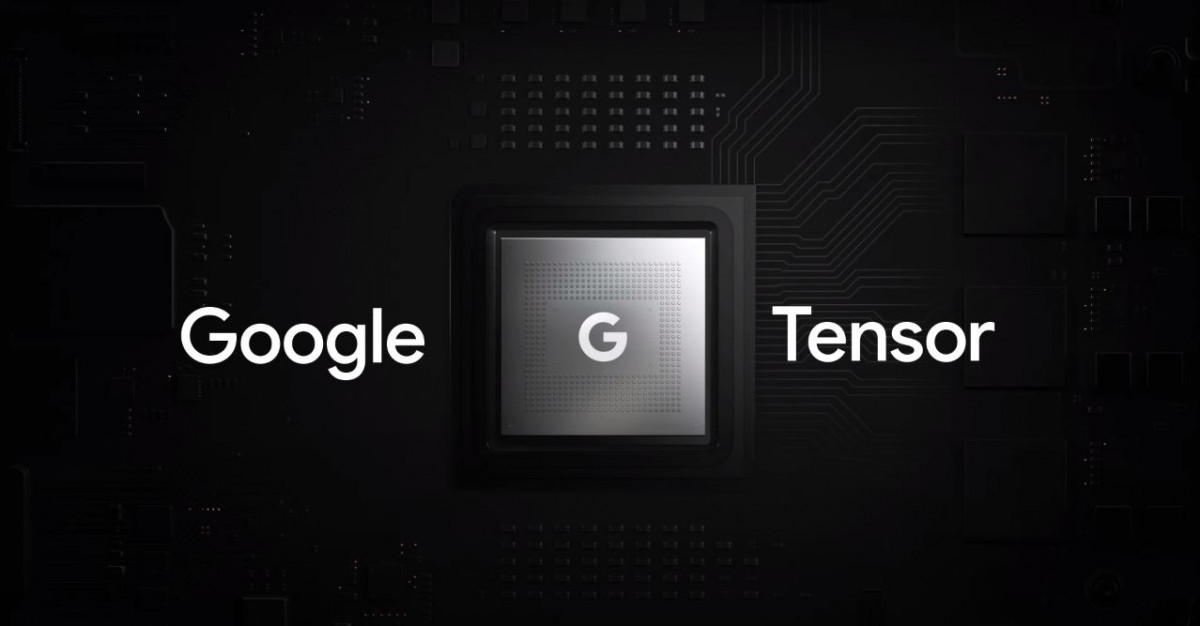
Google unveiled the Pixel 7 series last week but did not share detailed specs about the new Tensor G2 chipset. Earlier rumors pointed to a 4nm manufacturing process but as it turns out the new SoC is based on a 5nm process as a Google spokesperson confirmed to Android Authority.
We don’t get official confirmation if Tensor G2 is built on Samsung’s 5LPE process like the Tensor G1 or the newer 5LPP process. The confirmed specs for the Tensor G2 CPU includes 2x Cortex-X1 cores, 2x A78 and 4x A55 cores along with updates in clock speed while the GPU is a Mali-G710 MC10.
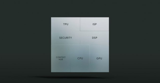
Google Tensor G2 chipset architecture
While a 5nm chipset may not deliver the same power efficiency as a 4nm chipset, Google’s new Tensor Processing Unit (TPU) is marketed as offering improved power efficiency as well as handling camera and machine learning tasks 60% faster than the Tensor G1's TPU.
Recommend
About Joyk
Aggregate valuable and interesting links.
Joyk means Joy of geeK